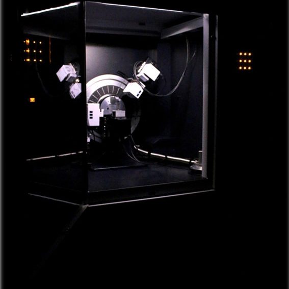
The Spectroscopy and Scattering Laboratory features equipment designed for the advanced characterization of nanomaterials based on spectroscopy and light scattering techniques. The laboratory provides equipment for X-ray diffraction (XRD), Raman spectroscopy, and X-ray photoelectron spectroscopy (XPS). The X-ray diffraction (XRD) technique is the main crystallographic analysis tool for determining the structure of materials, providing information on the spatial symmetry group, lattice parameters, and microstructure. Raman spectroscopy is an inelastic light scattering technique that uses a laser source to generate excitation photons, typically between UV and infrared, which, through the loss of energy to vibration modes in the sample, generate Raman scattering signals. This technique is very sensitive to changes in the local chemical structure and is used to examine the chemical bonds of materials. XPS is a surface chemical characterization technique. By using the photoelectric effect to excite the sample with X-rays, the spectroscopy of the photoelectrons emitted provides information on the elements present on the surface of the samples and the chemical states of these elements.
 Equipments
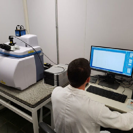
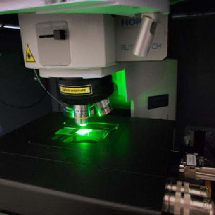
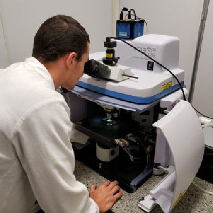
Confocal Raman Spectrometer (Horiba, XploRA™ plus)
Description: The confocal Raman spectroscopy technique allows the acquisition of specific mappings and Raman spectra (nano) materials, including assays temperature range -196 to 600 ° C. Coupling with the optical microscope allows us to obtain a visualization of particles or layers with dimensions below 1 micrometer with high magnification and spatial resolution, even in a three-dimensional (3D) configuration.
Specifications:
“• 3 lasers (473, 532 and 638 nm) and 6 power filters (0.1, 1.10.25, 50, 100%)
• CCD type detector (1024×256 pixels)
• Olympus BX optical microscope with 4 lenses (5, 10, 100x, and 50x LWD) and XYZ table attached to the equipment
• Accessory for temperature control for in situ analysis (-196 and 600 °C)
• Software for data acquisition and processing: LabSpec 6 with NavMap™, NavSharp and ViewSharp modules.
• Samples in liquid and solid state
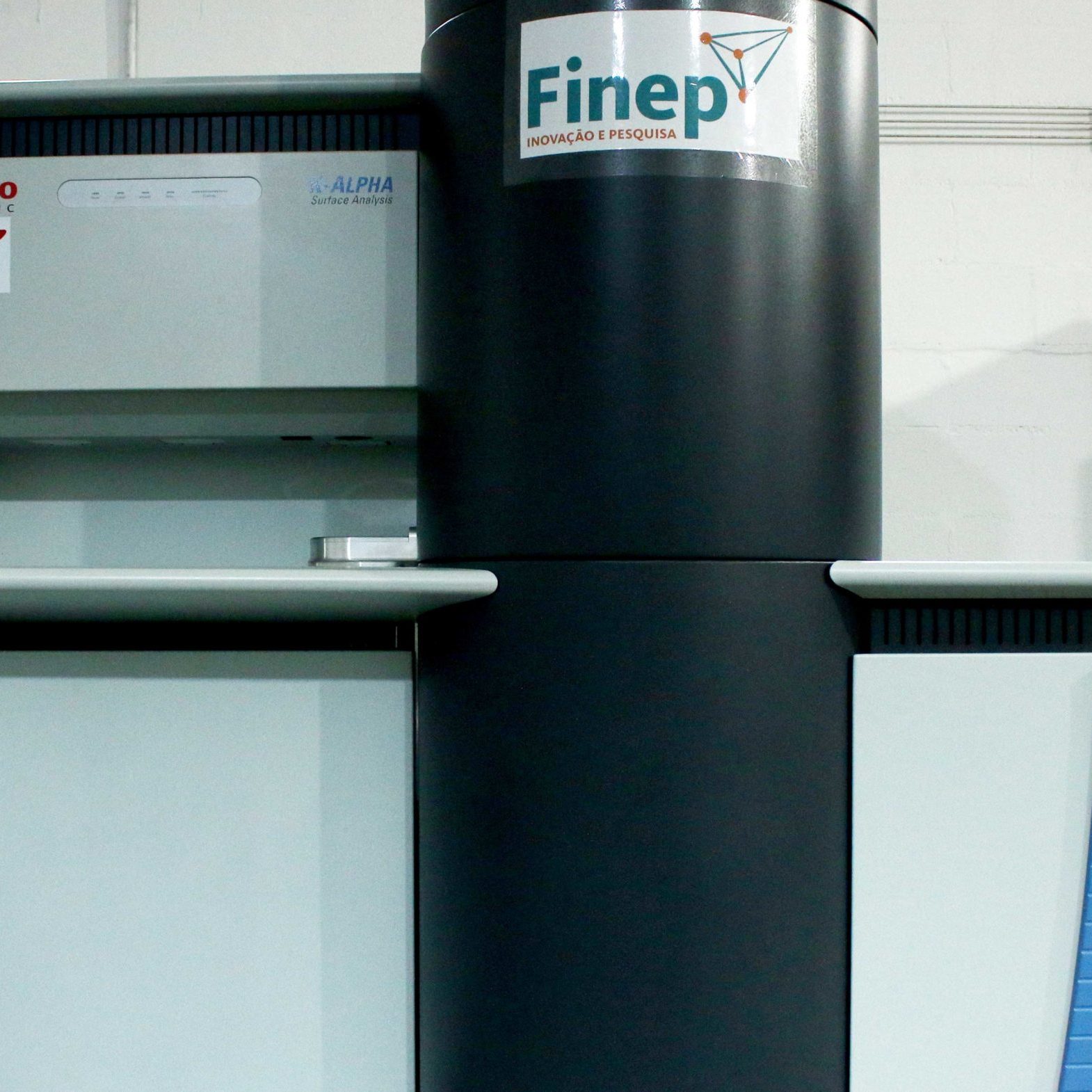
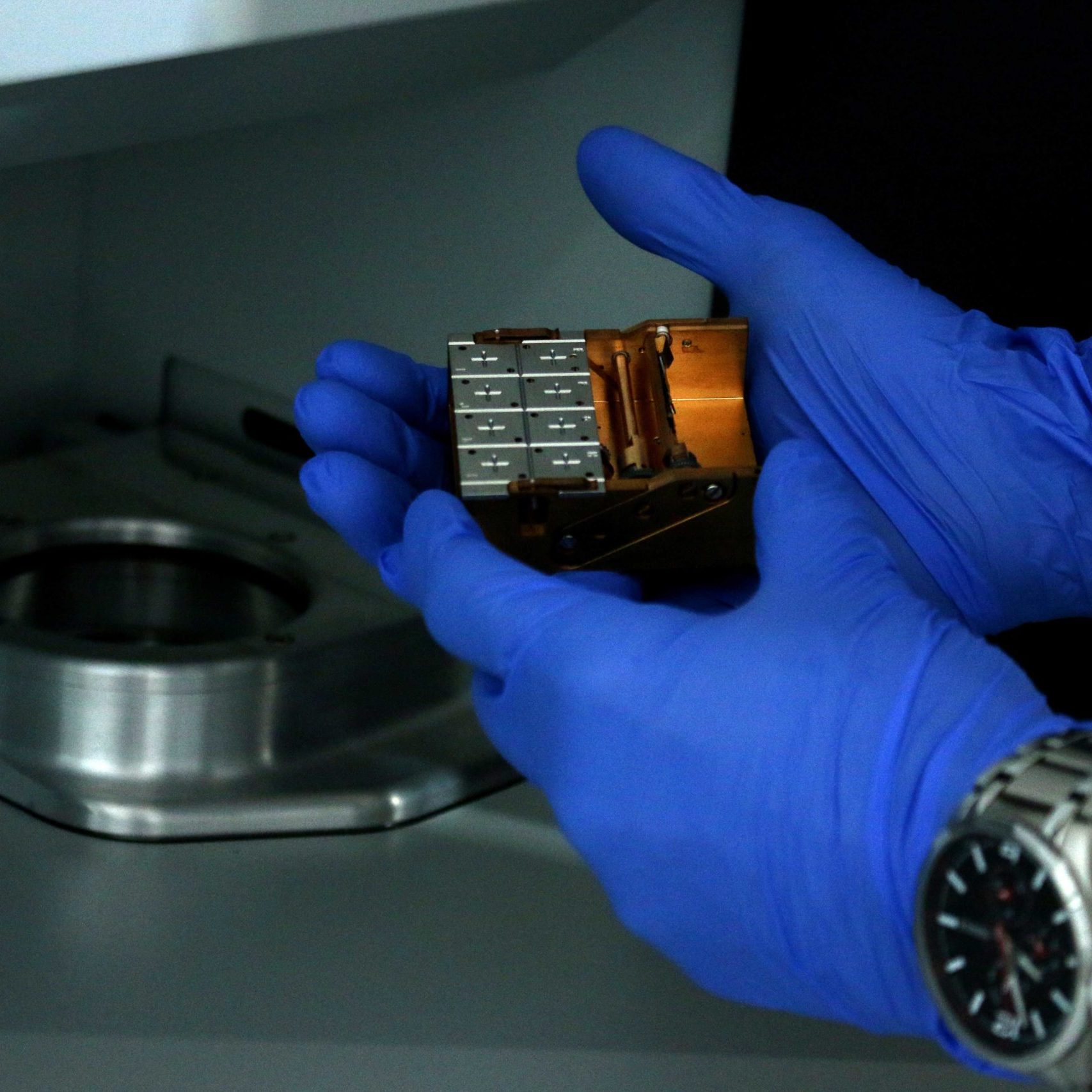
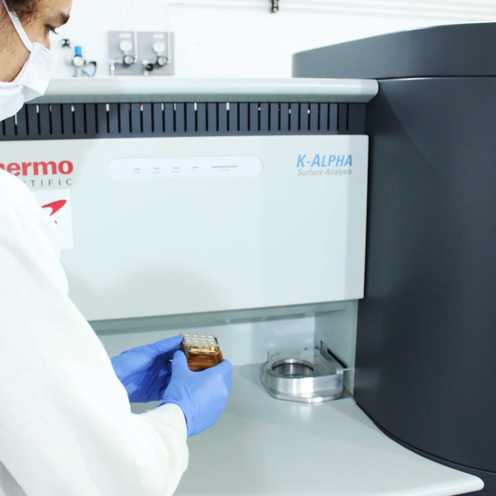
X-ray excited photoelectron spectrometer (XPS)
Description: The XPS technique is used for the chemical characterization of very thin surface layers in the order of 1-10 nm. It is based on the photoelectric effect. Briefly, the samples are irradiated with X-rays and the photoelectrons emitted by them are resolved as a function of their kinetic energies. Through the analysis of the spectra it is possible to obtain the elemental composition, the chemical and electronic state of the elements.
Specifications:
• X-ray source: Al Ka microfocus with variable spot size
• Analyzer: double focus hemispherical with 128 detection channels
• Ion cannon and ion cluster
• Load compensation system
• Avantage software for data acquisition and processing
• Maximum sample size: 60 mm (c) x 60 mm (w) x 20 mm (h)
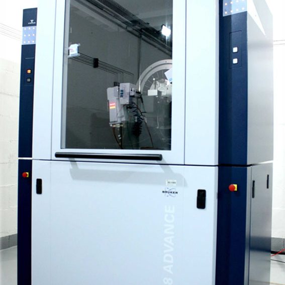
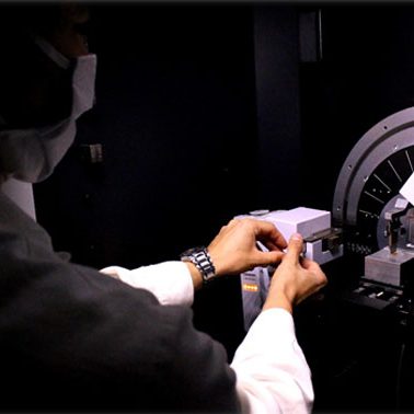
X-ray diffractometer (Bruker, D8 Advance Eco)
Description: The X-ray diffraction technique allows the identification of the crystal structure of materials, revealing details about unit cell parameters and its volume. Even with the database available, the crystallographic phase formed can be attributed from the indexing of the peaks, as well as obtaining information from preferred crystallographic orientations or texturing.
Specifications:
- Two radiation sources of Cu (8 keV, Qmax ≈ 8 Å-1) and Mo (17 keV, Qmax ≈ 17 Å-1).
- TRIO primary optics consisting of (1) Motorized Divergence Slit for Bragg-Brentano Geometry, (2) Göbel Mirror for parallel beam analysis, and (3) Germanium Monochromator for HRXRD with low divergence and presence of only Cu’s Kα.
- Four types of sample holders such as (1) rotation stage, (2) motorized table, (3) heating oven up to 1600 °C, and (4) capillary for transmission mode scattering techniques.
- TWIN secondary optics with (1) a motorized slit for Bragg-Brentano geometry and (2) an equatorial Soller for parallel beam geometry.
- LYNXEYE XE detector (point-0D and line-1D mode) requiring no kβ filter and allowing 100% removal of the Fe fluorescence signal using Cu radiation.
- Phase identification.
- Quantitative phase analysis.
- Microstructure analysis.
- Structure determination and refinement.
- Grazing Incidence Diffraction (GID).
- High-Resolution X-ray Diffraction (HRXRD).
- X-ray Reflectometry (XRR).
- Pair Distribution Function (PDF) analysis.
- Get to know the division
- Facilities
- In-situ Growth Laboratory (LCIS)
- Spectroscopy and Scattering Laboratory
- Photoelectrochemistry Laboratory
- Transmission Electron Microscopy Laboratory
- Scanning and Dual-Beam Electron Microscopy Laboratory
- Atomic Force Microscopy Laboratory
- Nanoceramics Processing Laboratory
- Nanomaterials Synthesis Laboratory
- Staff
- Contact us


