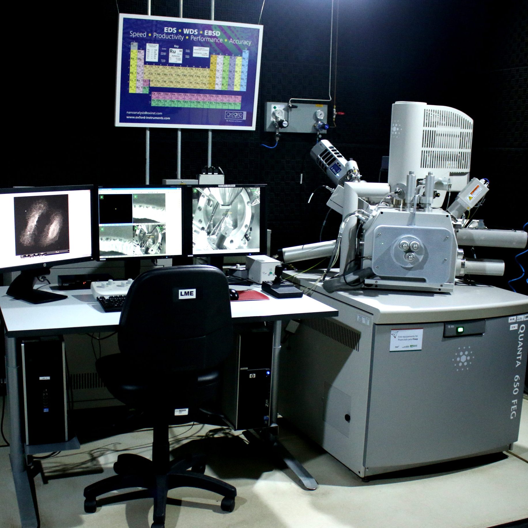
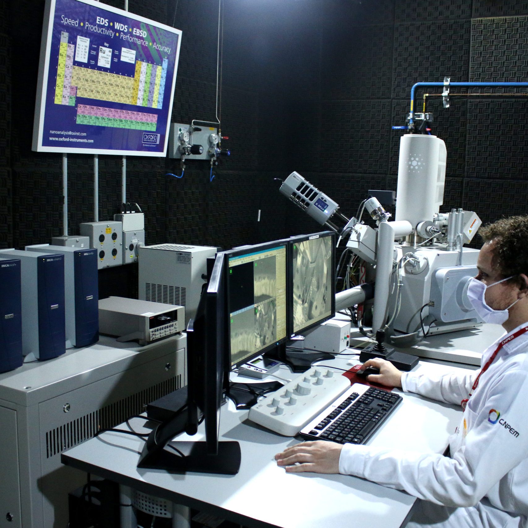
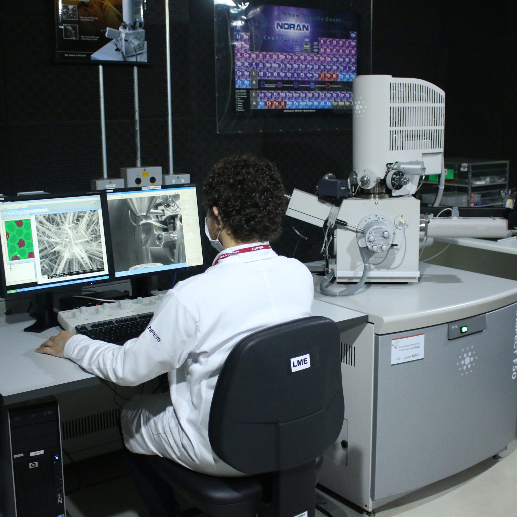
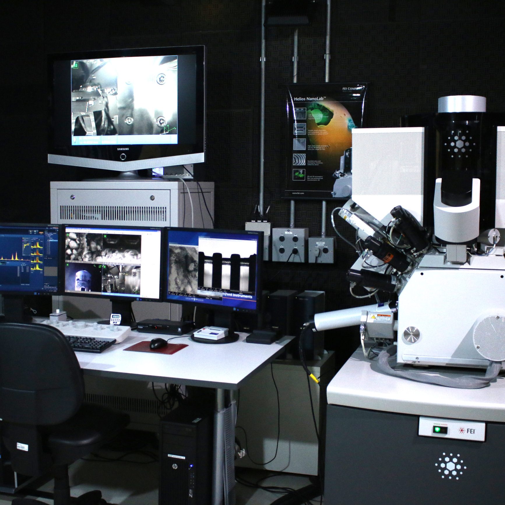
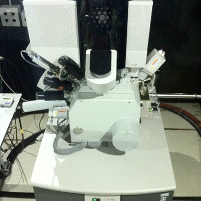
The Scanning Electron Microscopy and Dual-Beam Laboratory at LNNano offers the scientific community access to advanced characterization techniques using Scanning Electron Microscopy (SEM) and Double Beam (FIB). It features infrastructure for sample preparation and data processing, allowing for high-resolution image acquisition, chemical analysis by energy dispersive X-ray spectroscopy (EDS), crystallographic analysis by backscattered electron diffraction (EBSD), and transmitted electron diffraction (TKD), as well as advanced experiments such as in situ sample heating in the SEM and environmental mode scanning microscopy (ESEM). The laboratory’s double-beam electron microscopes also allow for the nanofabrication of structures and cuts for cross-sectional analysis, nanomanipulation of devices, deposition of micrometric structures of conductive and insulating materials, preparation of ultra-thin samples for transmission electron microscopy (TEM), and three-dimensional reconstructions by sequential cutting.
 Equipments
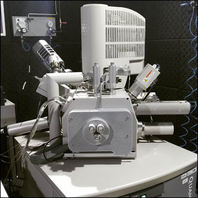
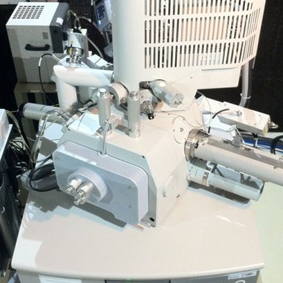
Thermo Fisher Scientific Quanta 650 FEG
Description: Scanning electron microscope with FEG Schottky electron gun and accelerating voltage between 500 V and 30 kV. It allows acquisition of secondary (SE), backscattered (BSE) and transmitted (STEM) electron images, with resolutions of 1.2 nm, 3.0 nm and 0.8 nm respectively. It can operate in high vacuum (HV), low vacuum (LV) and environmental (ESEM) modes, allowing the analysis of a wide variety of metallic, ceramic, polymeric, semiconductor and biological materials, as well as wet, liquid and non-conductive samples. It features detectors for energy dispersive X-ray spectroscopy (EDS), electron backscatter diffraction (EBSD), plasma cleaning to remove carbon contamination and heating device for in situ experiments at temperatures up to 1000 °C.
Specifications:
IMAGE ACQUISITION
SE (Secondary Electrons); BSE (Backscattered Electrons); STEM (Transmitted Electrons in Scan Transmission Mode – BF, DF and HAADF).
CHEMICAL ANALYSIS
EDS (Energy Dispersion X-ray Spectroscopy).
CRYSTALOGGRAPHIC ANALYSIS
EBSD (Backscattered Electron Diffraction); TKD (Kikuchi diffraction in transmission mode).
OTHER AVAILABLE TECHNIQUES
LV (Scanning Electron Microscopy in Low Vacuum Mode); ESEM (Scanning Electron Microscopy in Environmental Mode); Heating stage for in situ heating experiments up to 1000 °C; Integrated Plasma Cleaner.
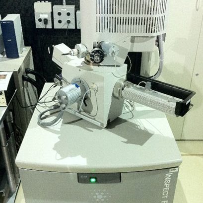
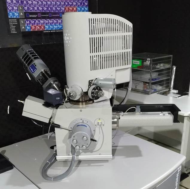
Thermo Fisher Scientific Inspect F50
Description: Scanning electron microscope with FEG Schottky electron gun and accelerating voltage between 500 V and 30 kV. It allows acquisition of secondary (SE), backscattered (BSE) and transmitted (STEM) electron images, with resolutions of 1.0 nm, 2.5 nm and 0.8 nm respectively. It operates only in high vacuum (HV) mode, but allows you to analyze with high resolution a wide variety of materials such as metals, ceramics, polymers and semiconductors. It has a detector for energy dispersive X-ray spectroscopy (EDS).
Specifications:
IMAGE ACQUISITION
SE (Secondary Electrons); BSE (Backscattered Electrons); STEM (Transmitted Electrons in Scan Transmission Mode – BF, DF and HAADF).
CHEMICAL ANALYSIS
EDS (Energy Dispersion X-ray Spectroscopy).
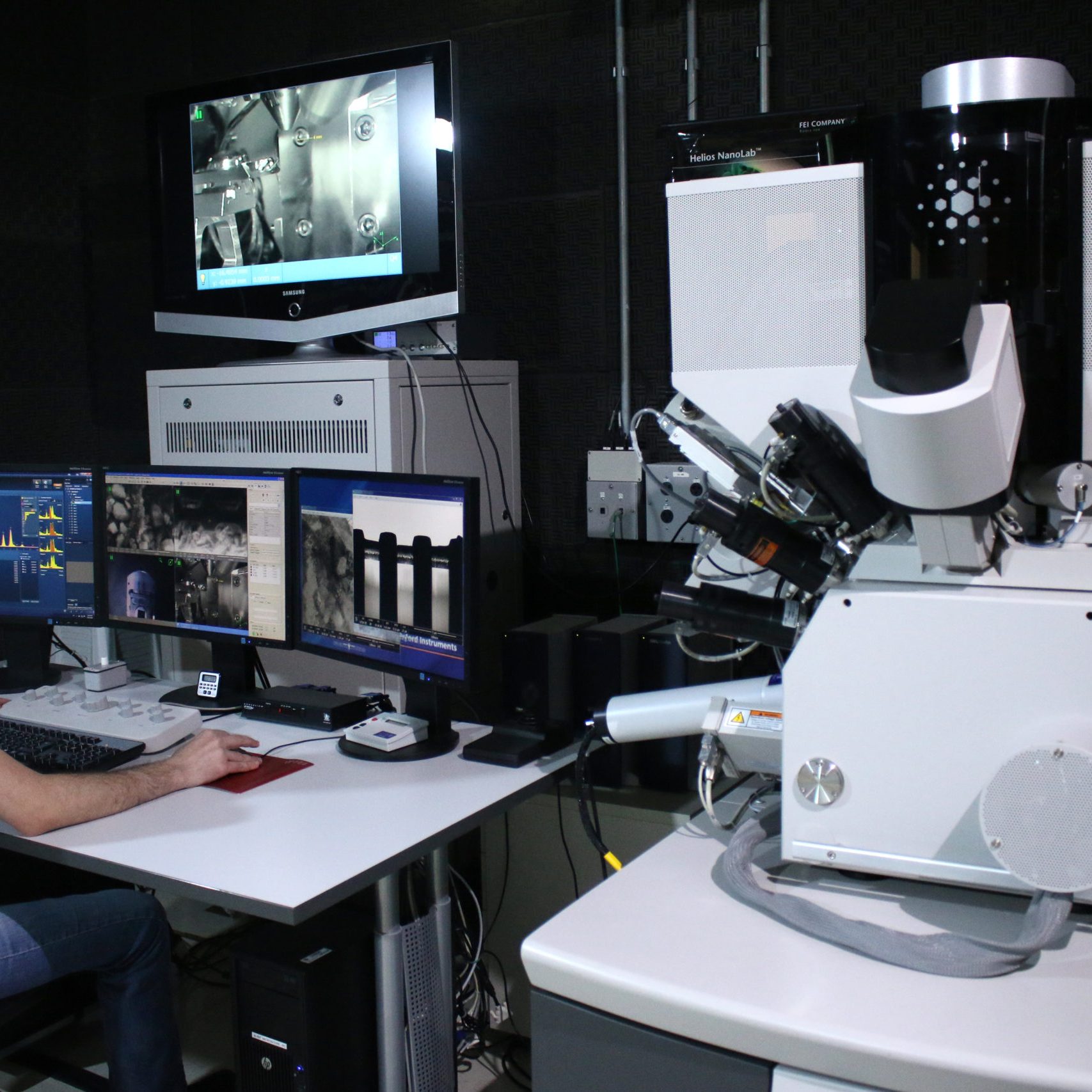
Thermo Fisher Scientific Helios NanoLab 660
Description: Double-beam electron microscope that combines a scanning electron microscope (SEM) with a focused ion beam microscope (FIB). It has FEG Schottky electron gun with accelerating voltage between 20 V and 30 kV and gallium ion gun with accelerating voltage between 500 V and 30 kV. It allows acquisition of secondary (SE), backscattered (BSE) and transmitted (STEM) electron images, with resolutions up to 0.6 nm. It has a nanomanipulator, immersion lens, monochromator, gas injection system (GIS) for deposition of materials, plasma and cryogenic sample cleaning devices, and detectors for energy dispersive X-ray spectroscopy (EDS) and electron backscattered diffraction (EBSD). It is an extremely versatile equipment that allows analysis with very high resolution (XHR), nano fabrication, preparation of ultra-fine samples for transmission electron microscopy and 3D reconstructions by sequential cuts.
Specifications:
SE (Secondary Electrons); BSE (Backscattered Electrons); STEM (scanning transmission electron microscope – BF, DF and HAADF).
CHEMICAL ANALYSIS
EDS (Energy Dispersion X-ray Spectroscopy).
CRYSTALOGGRAPHIC ANALYSIS
EBSD (electron backscatter diffraction); TKD (transmission Kikuchi diffraction).
FIB (FOCUSED ION BEAM) TECHNIQUES.
Nanofabrication and Cross Section Analysis; Deposition of nanostructures (Pt, TEOS, C); Preparation of ultra-fine samples for TEM (FIB-Lamela); 3D reconstructions by sequential cuts (FIB Tomography).
- Get to know the division
- Facilities
- In-situ Growth Laboratory (LCIS)
- Spectroscopy and Scattering Laboratory
- Photoelectrochemistry Laboratory
- Transmission Electron Microscopy Laboratory
- Scanning and Dual-Beam Electron Microscopy Laboratory
- Atomic Force Microscopy Laboratory
- Nanoceramics Processing Laboratory
- Nanomaterials Synthesis Laboratory
- Staff
- Contact us


