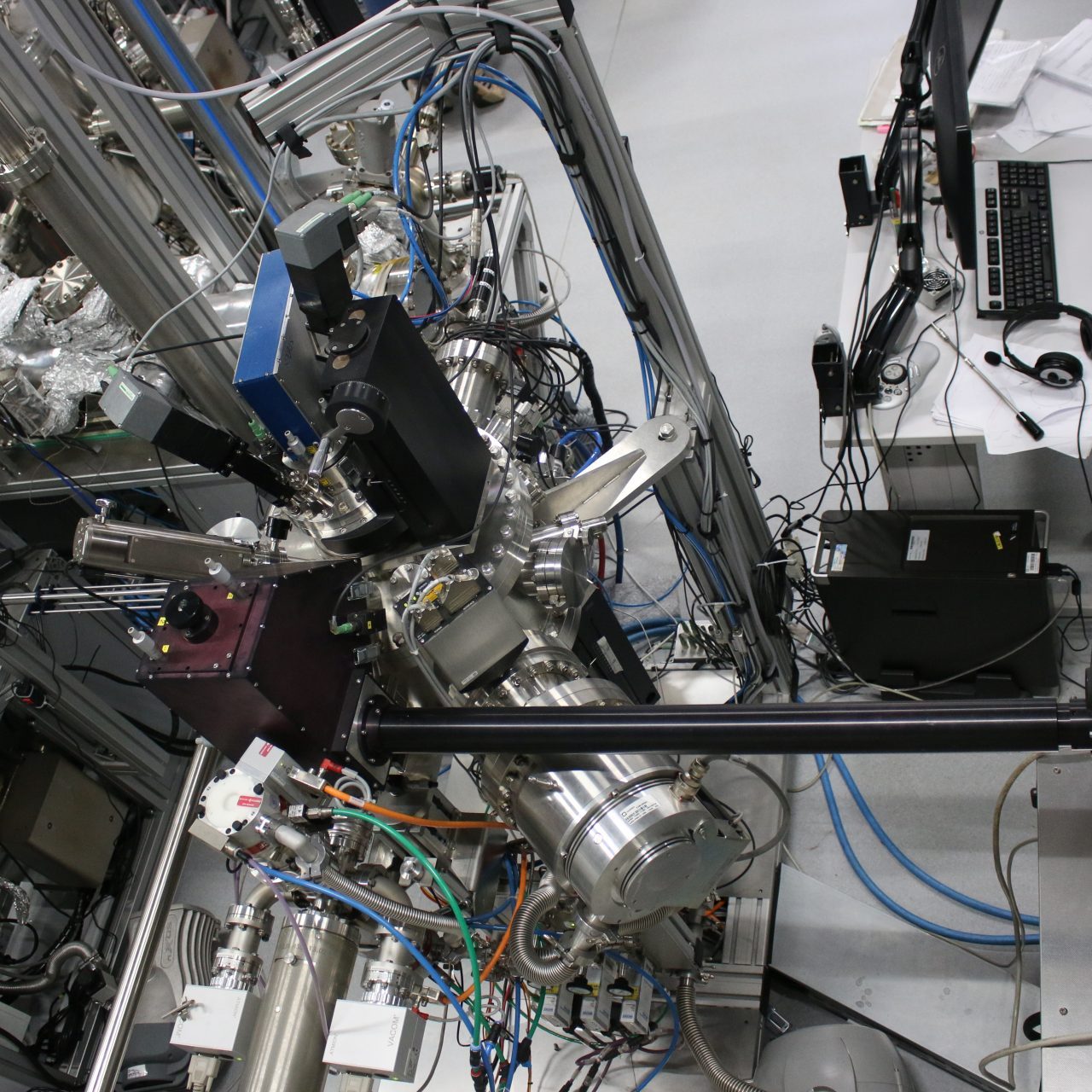
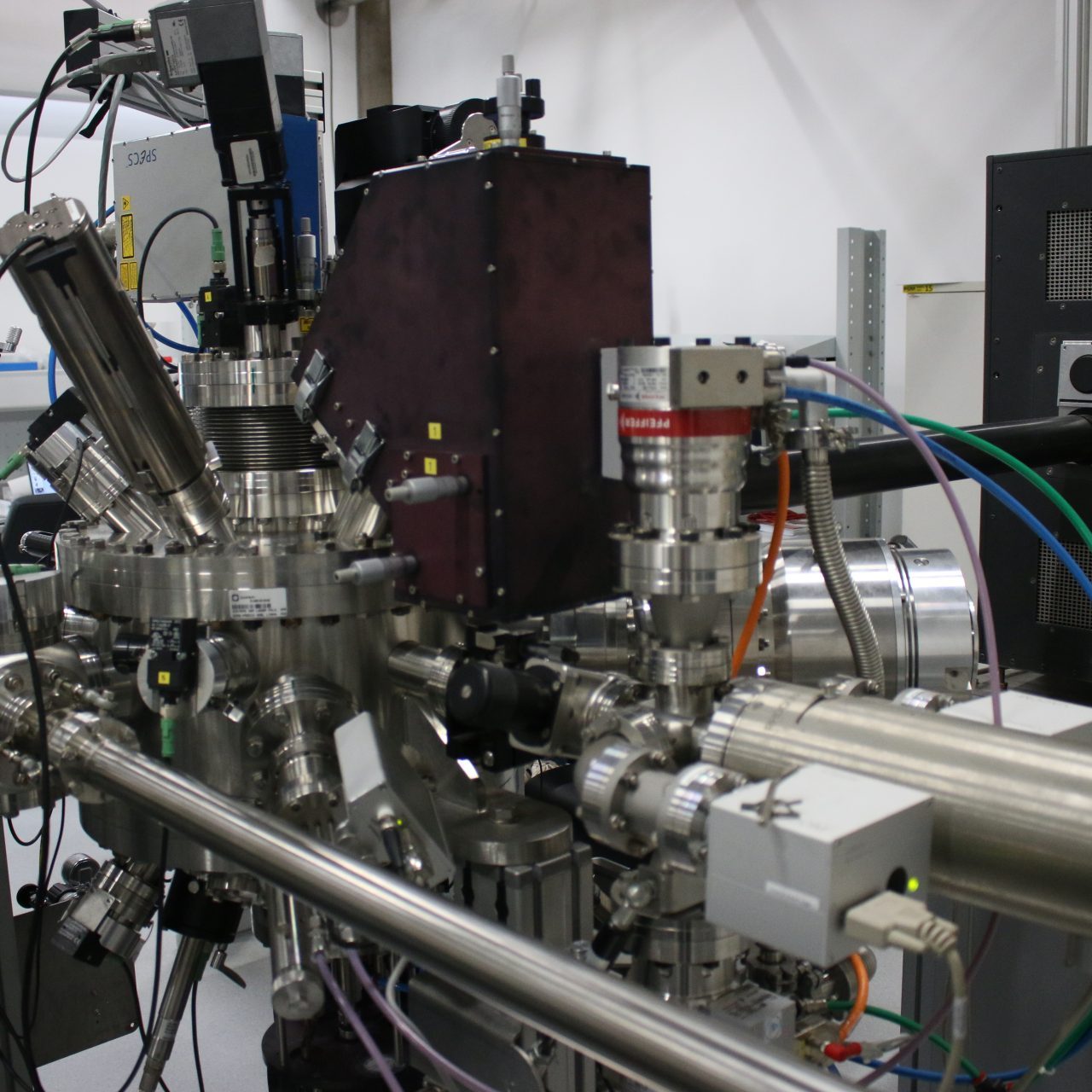
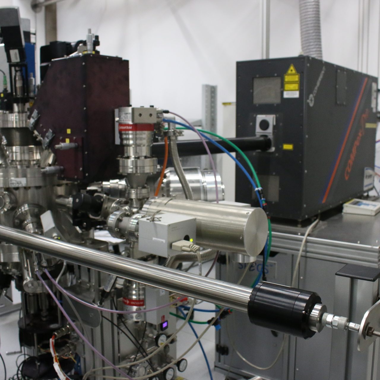
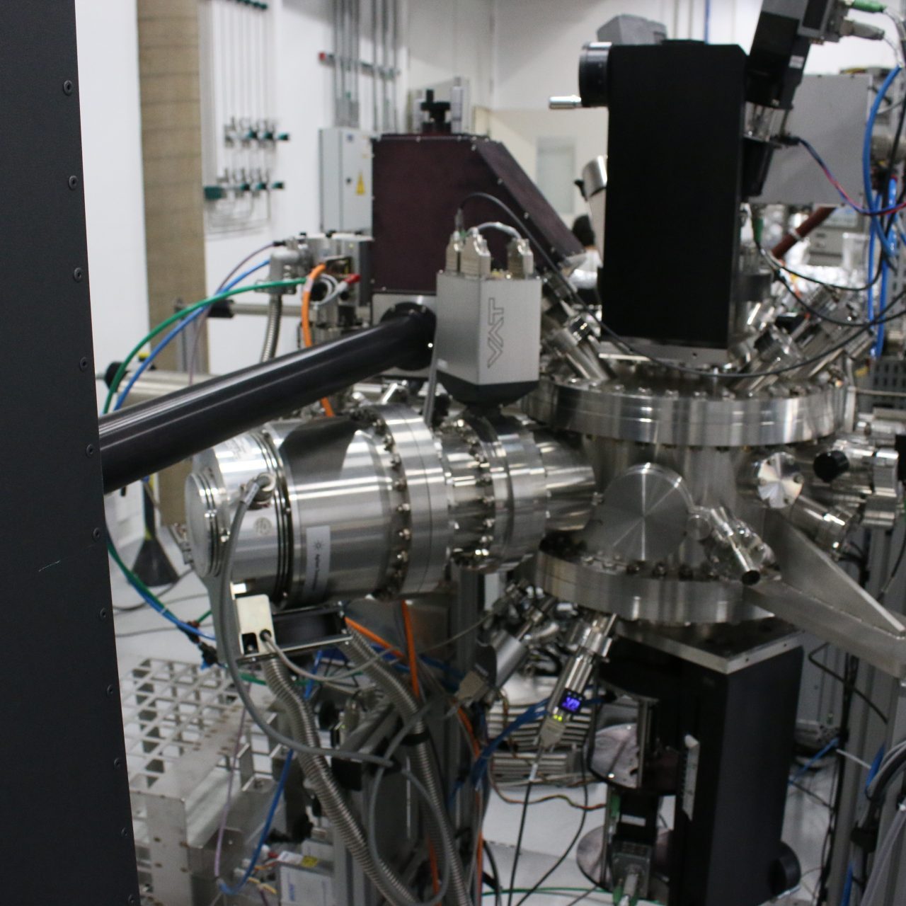
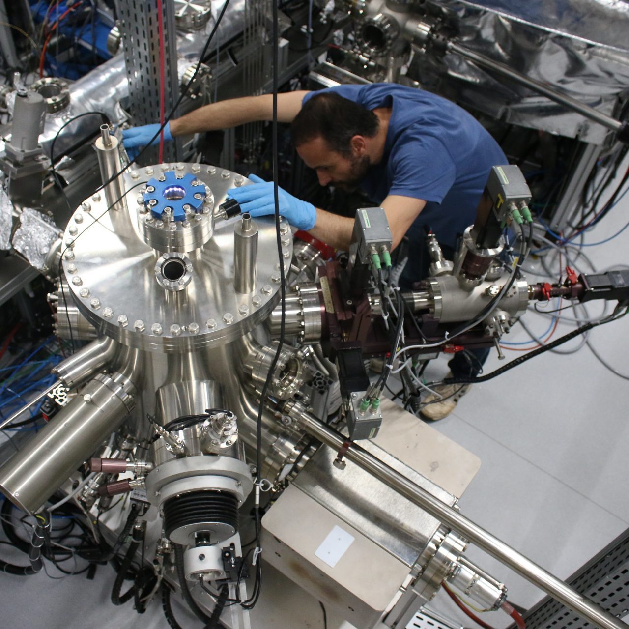
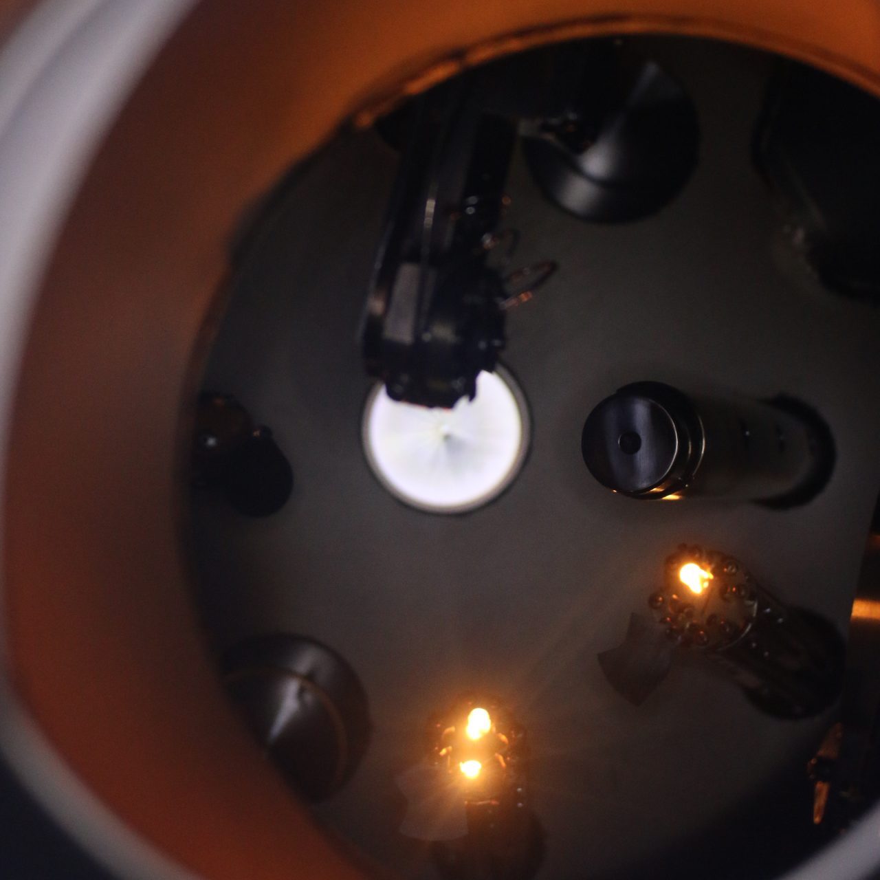
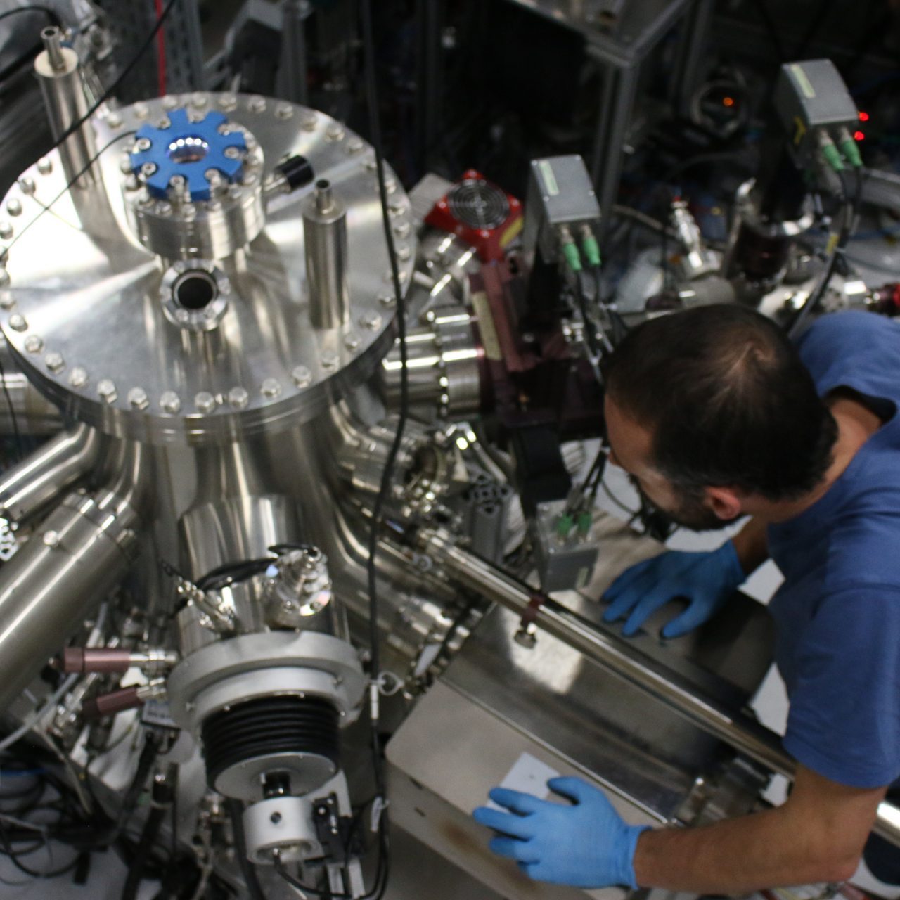
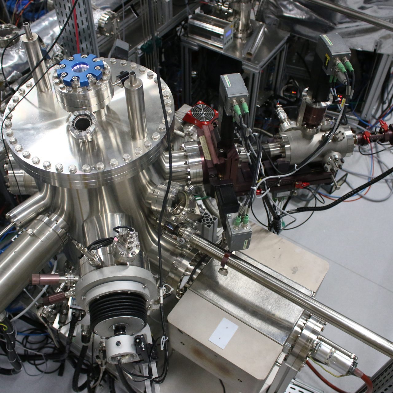
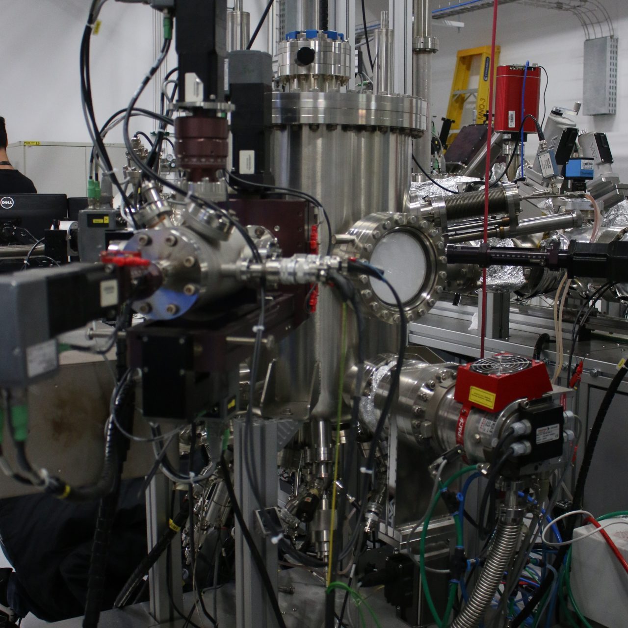
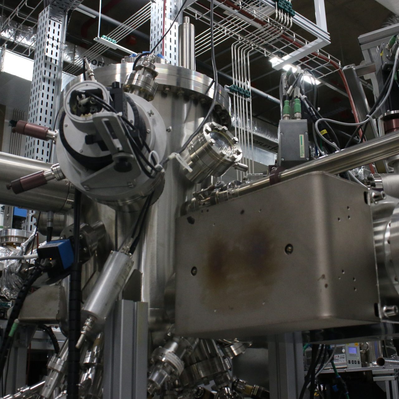
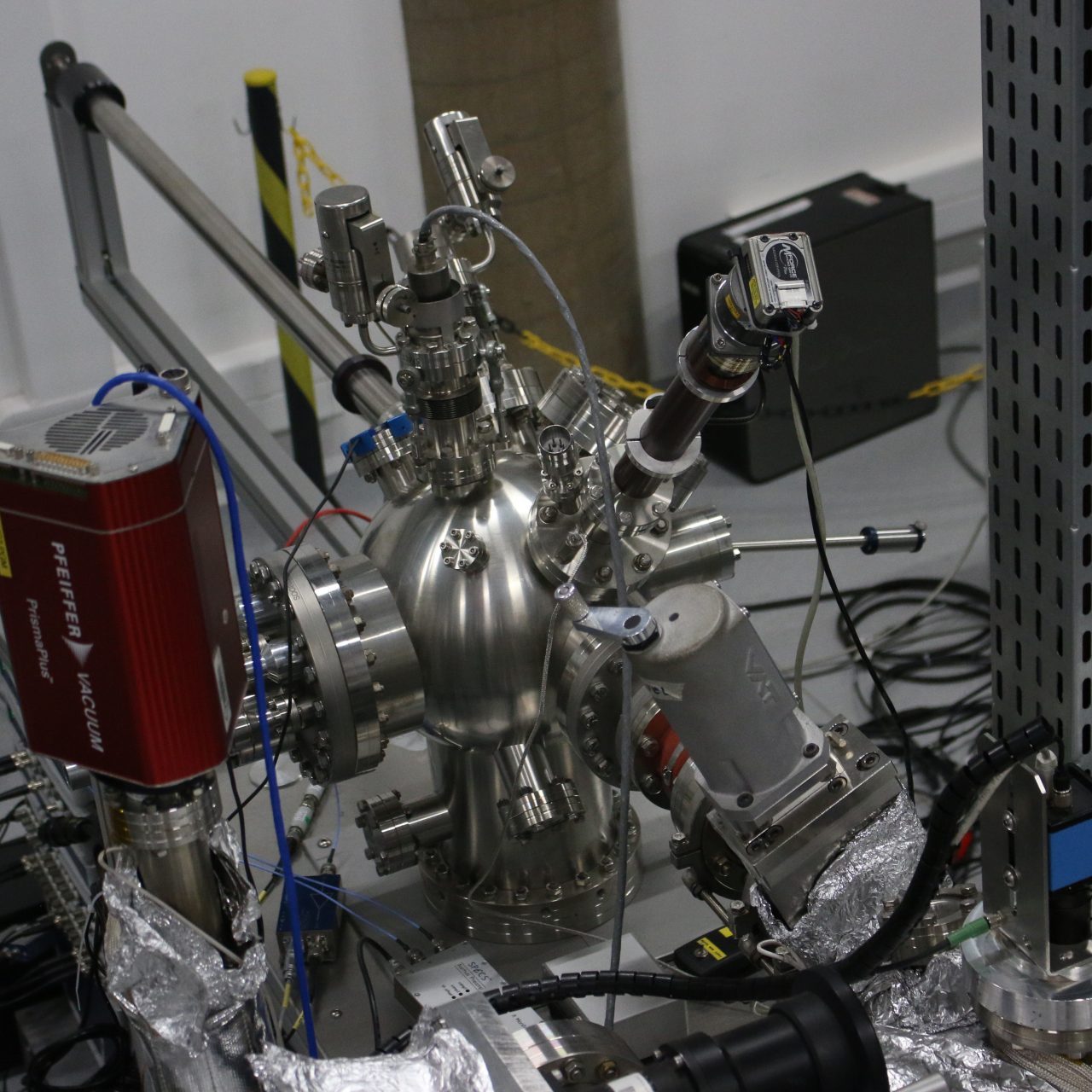
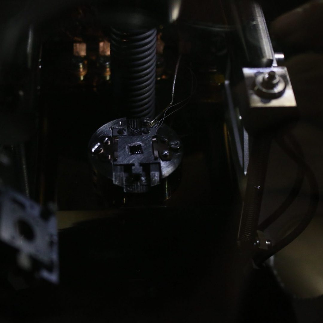
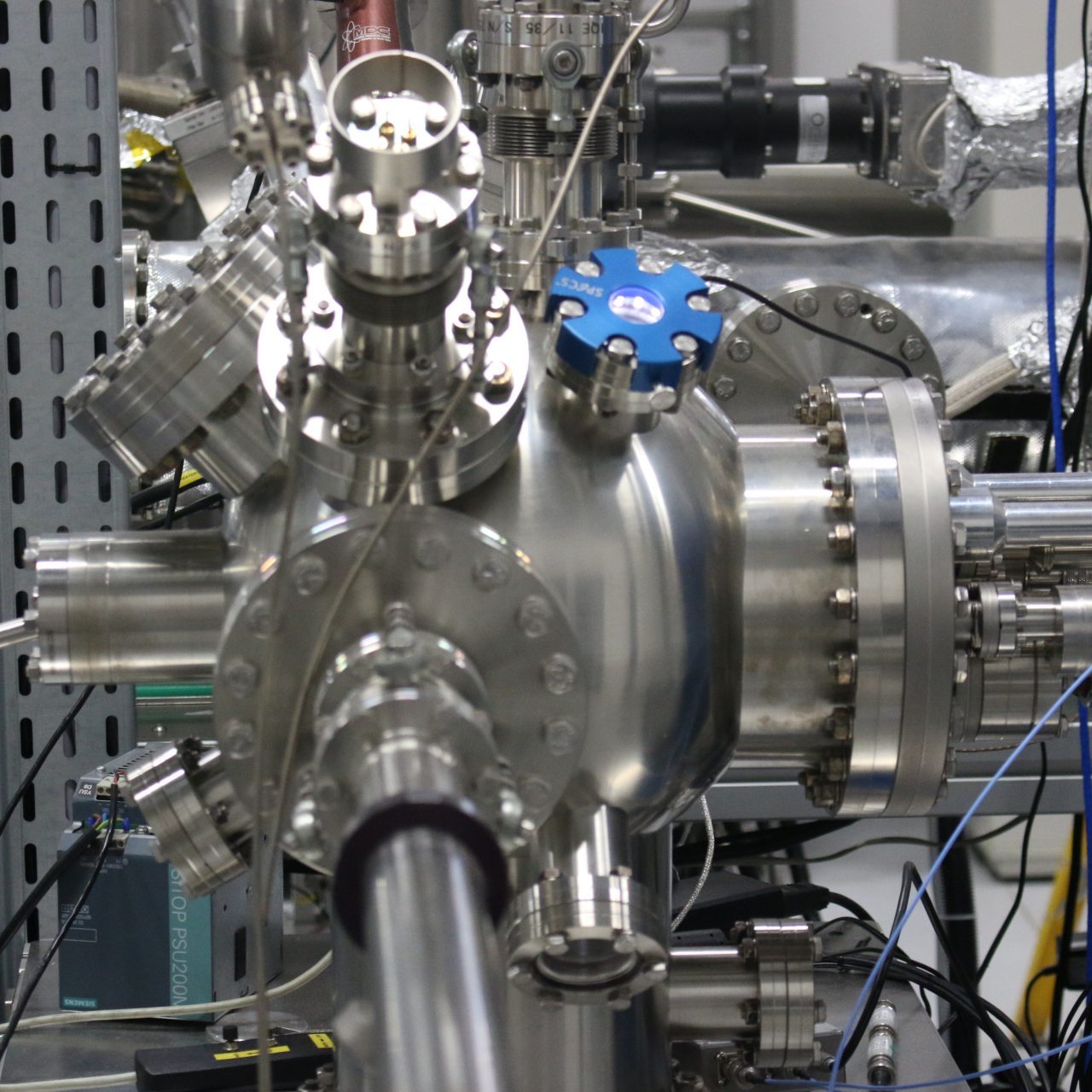
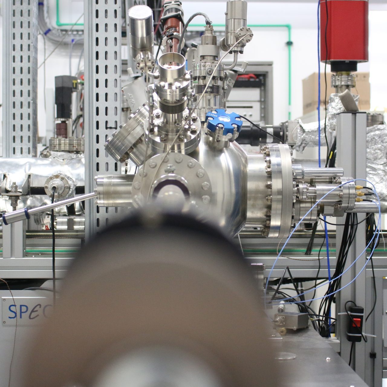
The In-Situ Growth Laboratory (LCIS) provides state-of-the-art tools for the growth of thin films and heterostructures for further studies with synchrotron radiation, electron microscopy, or other advanced techniques at CNPEM. The available growth techniques are based on physical vapor deposition in the modes of pulsed laser deposition (PLD) and molecular beam epitaxy (MBE). They can grow films of transition metals, oxides, and some simple organic molecules. It is possible to transport the samples produced in an ultra-high vacuum environment to some of the Sirius beamlines, which is key to studying the surface of the films. The growth chambers are coupled via a tunnel that allows transfer between the different chambers in an ultra-high vacuum environment.
 Equipments
PULSED LASER DEPOSITION
Description: Pulsed laser deposition is a thin film growth technique that uses a high-power pulsed laser to pulverize and ionize the material of a target to be deposited. By shining the laser on a target of a certain material, a light plume is created which is directed at a substrate. This plume is composed of ions, neutral particles, and electrons, preserving the target’s stoichiometry under certain conditions. Being able to preserve the target’s stoichiometry is a major advantage of this technique. It also allows deposition to be achieved in a controlled atmosphere (from vacuum to a few mbar). PLD has been used as a technique for growing films of various materials such as superconducting cuprates and ferroelectric or ferromagnetic oxides.
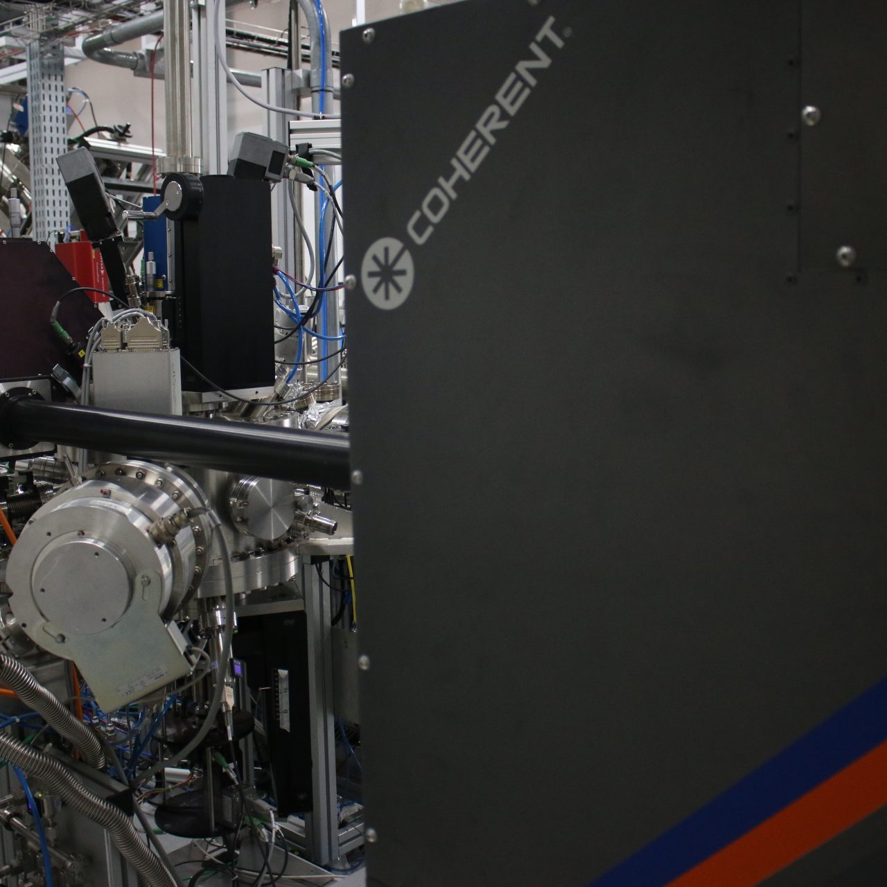
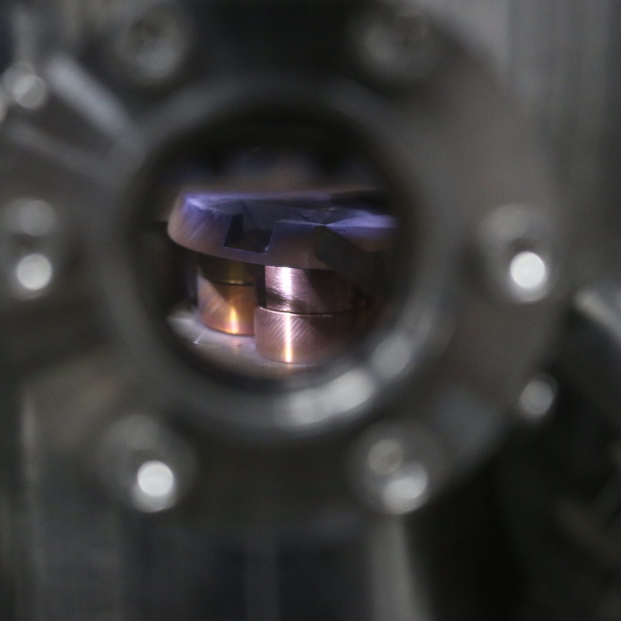
Technical features: The LCIS is equipped with a pulsed laser deposition chamber using a KrF Excimer laser with a wavelength of 248 nm, a maximum pulse energy of 400mJ, and a repetition rate of up to 20Hz. The deposition chamber contains a carousel with up to 6 targets with a diameter of 1 inch and a thickness of between 3 and 6 millimeters. The substrate carrier can be heated via infrared laser to 850°C. The deposition process can be performed at pressures between 1e-8mbar and 1mbar with a Nitrogen, Argon, or Oxygen atmosphere. The chamber is equipped with a quartz scale to calibrate the growth rate, and an electron gun to monitor growth via RHEED. The targets can be brought in by users as long as the chemical composition does not contain highly volatile atoms (Pb, K).
MOLECULAR-BEAM EPITAXY
Description: Molecular beam epitaxy is a technique for depositing films of high quality and crystallographic purity on suitable substrates. The technique is based on heating a target material to produce an atomic/molecular beam which, given the ultra-high vacuum conditions of the chamber, can move around the chamber until reaching a substrate and being incorporated. The growth rate is generally low, allowing the deposition to be controlled in the order of atomic layers.
Technical features: The LCIS has two chambers that use this technique: (i) one for LEED and RHHED, which even allows for monitoring the growth of transition metals (or materials with low vapor pressure) and (ii) another chamber adapted for the growth of organic molecules.
MBE FOR TRANSITION METALS (LOW VAPOR PRESSURE) – MBE-1
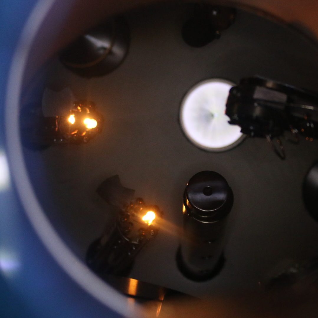
The chamber operates at a base pressure of 10-10 mbar, with 10 evaporators with electron beam heating and a quartz scale for calibrating the deposition rate. It is equipped with a system for thinning the substrate using argon ions (sputtering); it also allows the substrate to be heated using an electron beam. The substrates and films can be characterized in situ using electron diffraction optics in layer-by-layer growth mode. The system has a motorized mask for partial coverage of the substrate which may be used for wedge growth.
CHAMBER FOR THE DEPOSITION OF SMALL ORGANIC MOLECULES – O-MBE
The LCIS offers a deposition chamber equipped with a Knudsen evaporator for evaporating small organic molecules. The system can heat the substrate to 500°C and has a set of masks for selecting the deposition area. Evaporators brought in by users of some materials previously approved by the LNLS can be installed in this chamber.
SCANNING PROBE MICROSCOPY
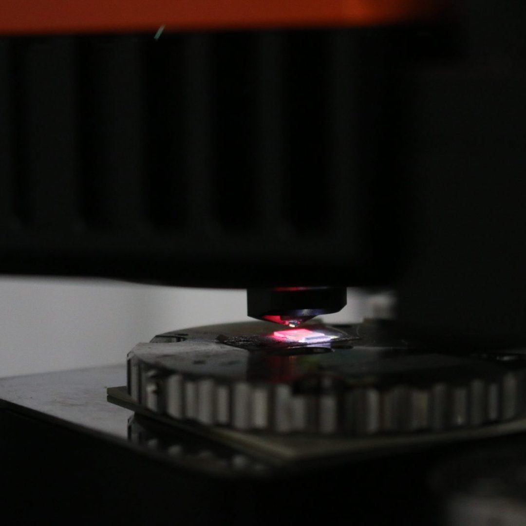
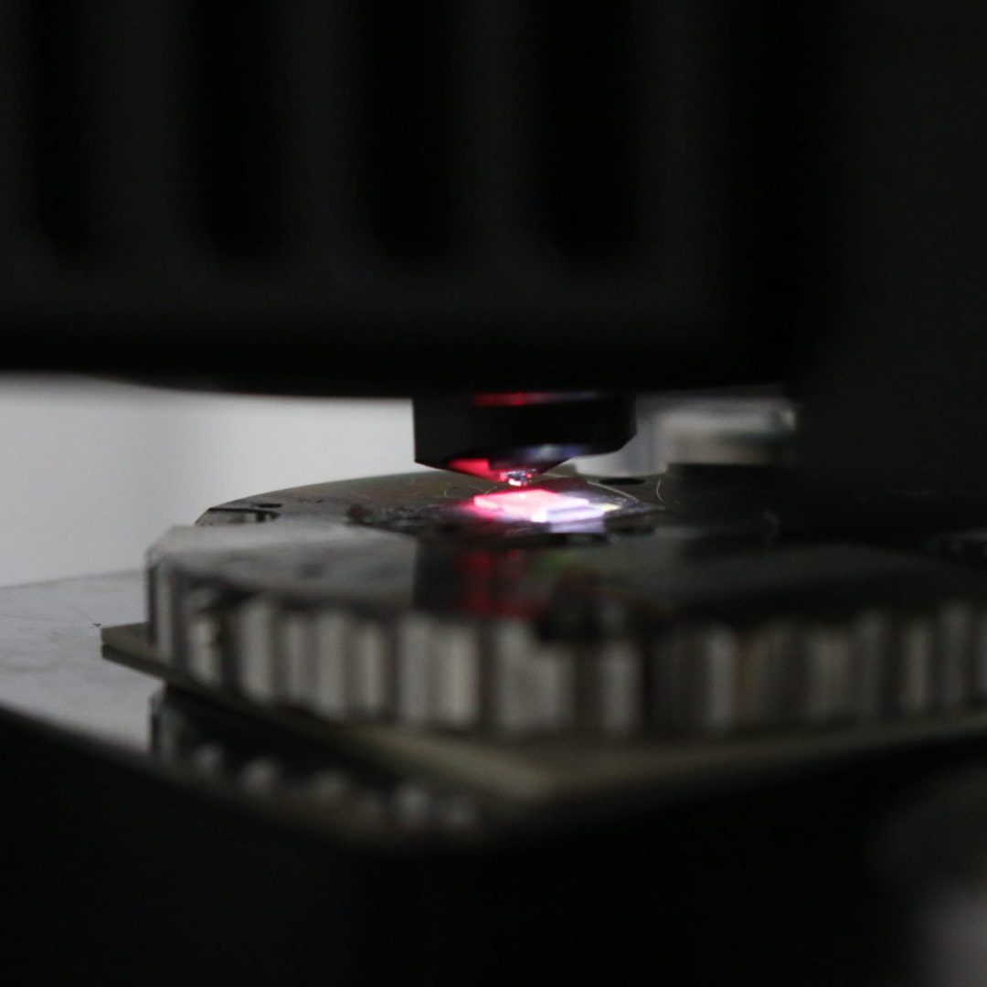
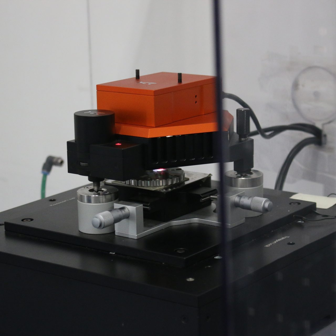
Description: The surface morphology of grown substrates or films can be researched using scanning probe microscopy. For such purposes, a small probe with a very sharp tip is used to scan the surface of the sample over a minimum distance. STM (Scanning Tunneling Microscopy) detects the tunneling current between the probe and the conductive sample, which is only significant once the distance between the probe and sample is very small. In AFM, the probe may be in contact with the sample, but in most cases, it is at a very small distance, around a few nanometers. Under these conditions, significant forces result from the probe’s interactions with the atoms or molecules on the surface.
Technical features: The LCIS features two microscopes to serve users. One of the microscopes operates in an ultra-high vacuum and is coupled to the growth chambers via a tunnel. It is a NANONIS microscope that uses Kolibri technology (KolibriSensor) allowing measurements in AFM or STM mode. Another microscope operates at atmospheric pressure. It is a Nanosurf FlexAFM that can operate in Atomic Force Microscopy, Piezo-Response Force Microscopy, Magnetic Force Microscopy, and Kelvin probe force microscopy modes.
- Get to know the division
- Facilities
- In-situ Growth Laboratory (LCIS)
- Spectroscopy and Scattering Laboratory
- Photoelectrochemistry Laboratory
- Transmission Electron Microscopy Laboratory
- Scanning and Dual-Beam Electron Microscopy Laboratory
- Atomic Force Microscopy Laboratory
- Nanoceramics Processing Laboratory
- Nanomaterials Synthesis Laboratory
- Staff
- Contact us


