The Microfabrication and Microfluidics Laboratory is designed to develop micrometric-scale devices and processes. It features an ISO 7-class clean room of 30m2 and an area for processes of 190m2 with photolithography equipment (UV and laser pattern generator), humid corrosion processes, physical vapor deposition (PVD) by electron beam and sputtering DC/RF, 3D printing (Fused Deposition Modeling – FDM and Stereolithography – SLA), sample inspection and metrology (optical microscopes and profilometer). The lab can develop devices such as microelectromechanical systems (MEMS), microfluidic devices (lab-on-a-chip), optical sensors, chemical sensors (colorimeters, separation, detection–amperometric and voltammetric), displacement sensors (MEMS accelerometers), and RF devices (THz, SAW, and RFID filters).
 Equipments
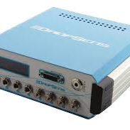
μstat 4000P – Dropsens
Specifications
Multichannel with up to 4 working electrodes, sharing an auxiliary and a reference electrode;
Voltammetric or amperometric measurements;
Potential range: +/- 4V;
Maximum current: +/- 80 Ma;
Current ranges: 1 nA to 100 mA;
PC interface: USB and Bluetooth®;
Battery powered.
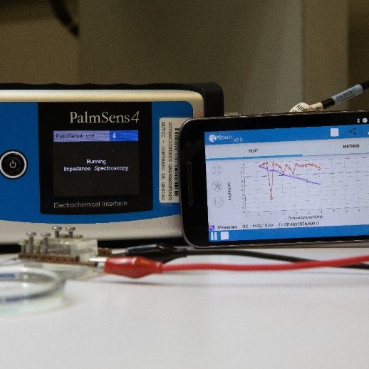
Potentiostat / Galvanostat / Impedance Analyzer
Specifications
Voltammetric, pulsed, amperometric, galvanostatic and impedance measurements;
FRA / EIS: 10 μHz to 1 MHz;
DC potential range: ± 10 V;
Maximum current: ± 30 mA;
Current range: 100 pA to 10 mA;
Interface for PC and smartphone: Bluetooth® or USB connection
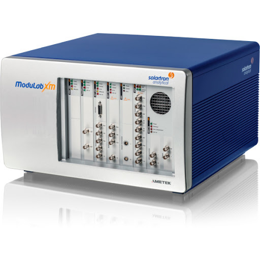
Impedance Analyzer
Specifications
Modules: MFRA 1MHz, MREF, MAT 1MHz;
Maximum DC voltage: ± 8 V;
Maximum current: ± 100 mA;
Maximum resolution: 1 μV;
FRA: 10 μHz to 1 MHz;
PC interface: 100BASE-T Ethernet.
- Get to know the division
- Facilities
- In-situ Growth Laboratory (LCIS)
- Spectroscopy and Scattering Laboratory
- Photoelectrochemistry Laboratory
- Transmission Electron Microscopy Laboratory
- Scanning and Dual-Beam Electron Microscopy Laboratory
- Atomic Force Microscopy Laboratory
- Nanoceramics Processing Laboratory
- Nanomaterials Synthesis Laboratory
- Staff
- Contact us


