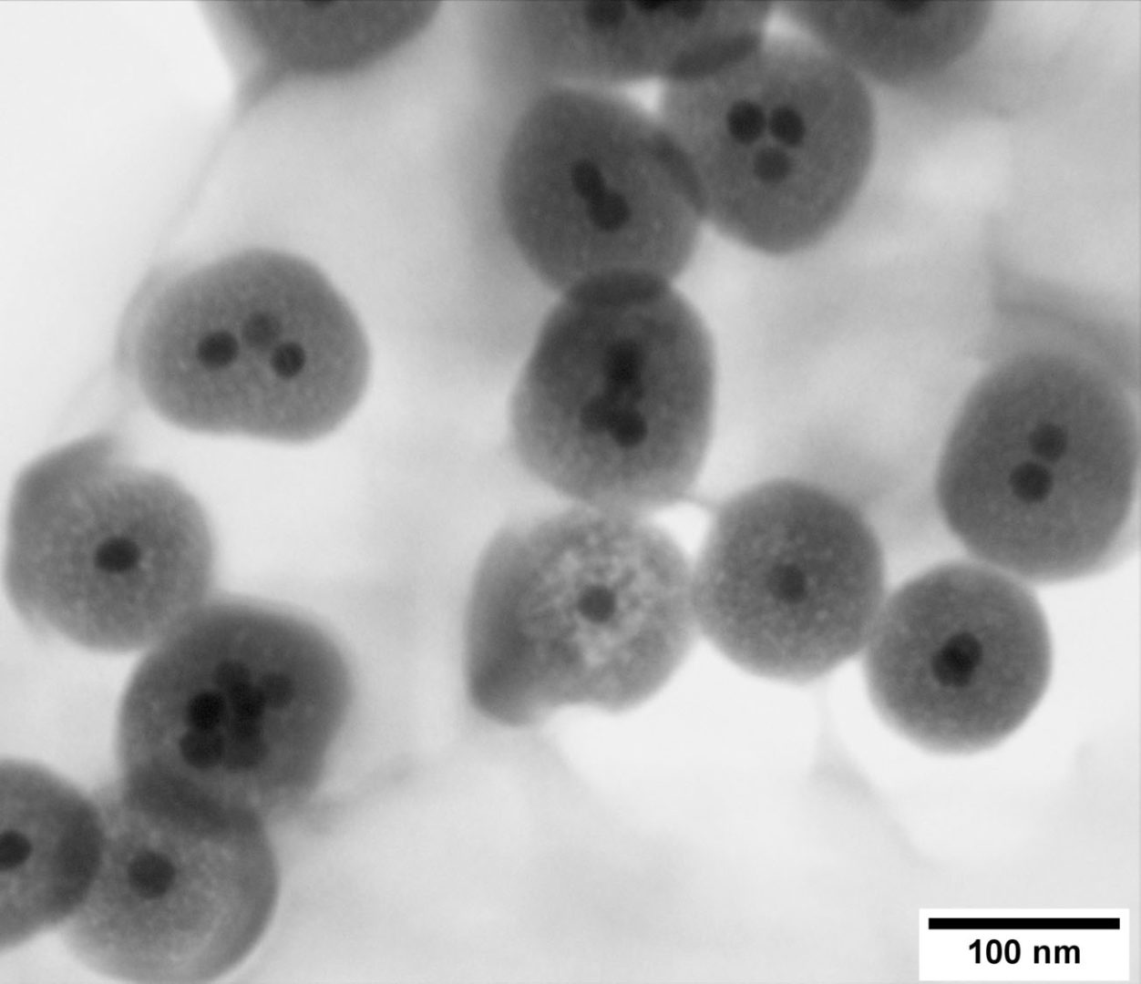
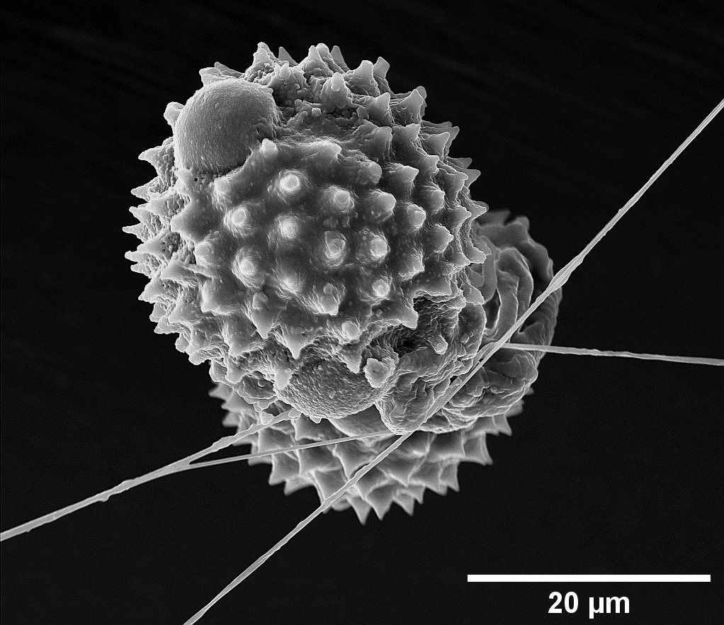
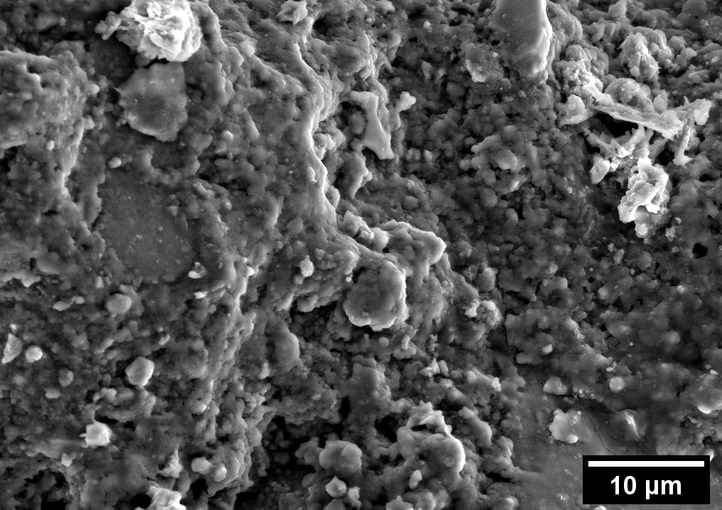
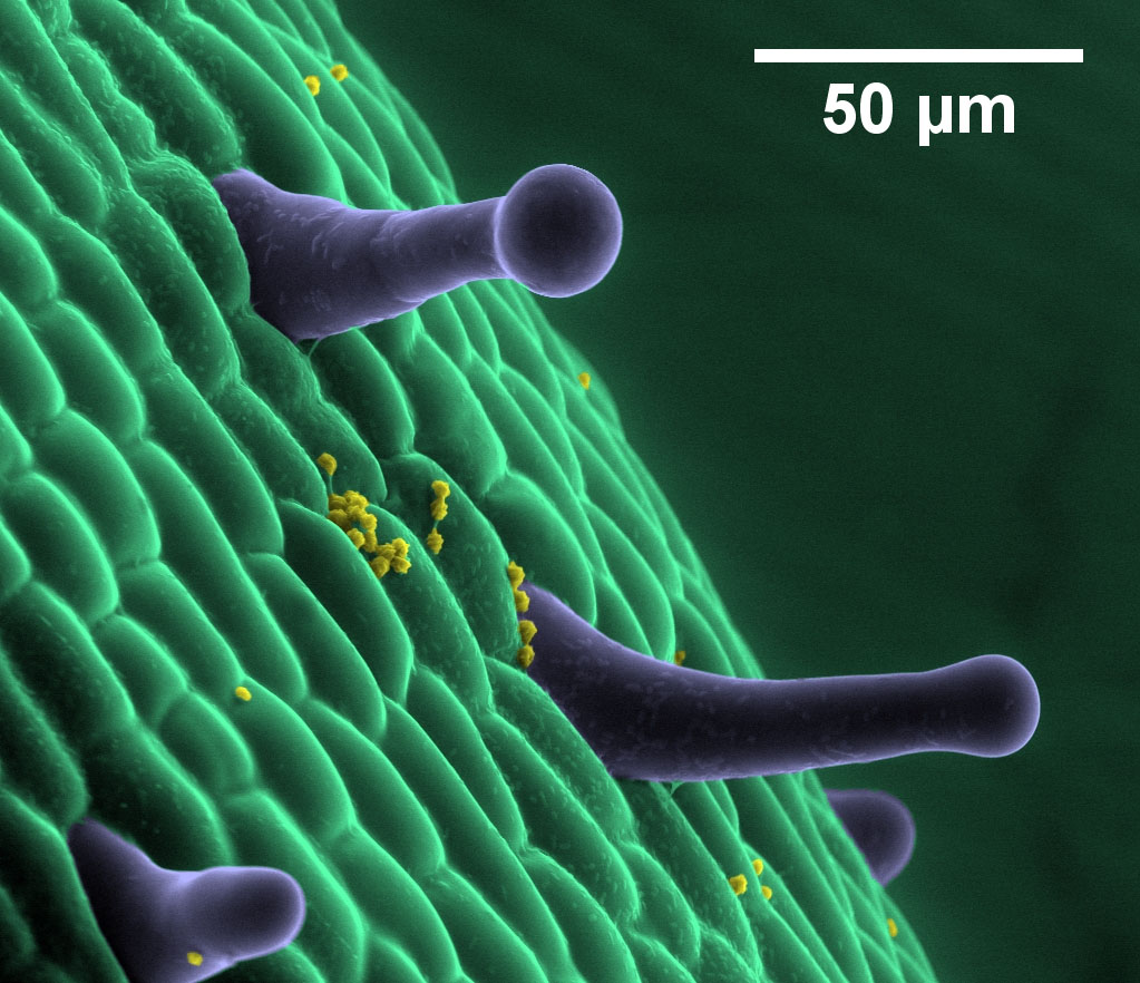
The crystallographic structure of materials, as well as their chemical composition and the binding states of the constituent chemical elements are routinely analyzed and visualized in electronic microscopes at atomic, nanometric and micrometric levels. Technological advances over the last few decades also allow the observation and analysis in situ of dynamic phenomena with increasing precision and reproducibility in atomic and nanometric dimensions.
LNNano provides the national and international scientific community with alternatives for accessing a wide range of conventional and advanced techniques of scanning, transmission and double-beam electron microscopy.
Infrastructure
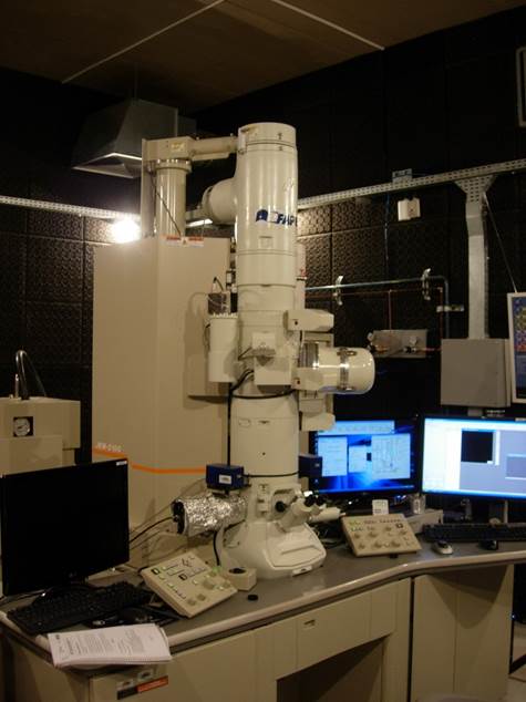
JEOL JEM-2100
JEOL JEM-2100
JEOL JEM-2100F
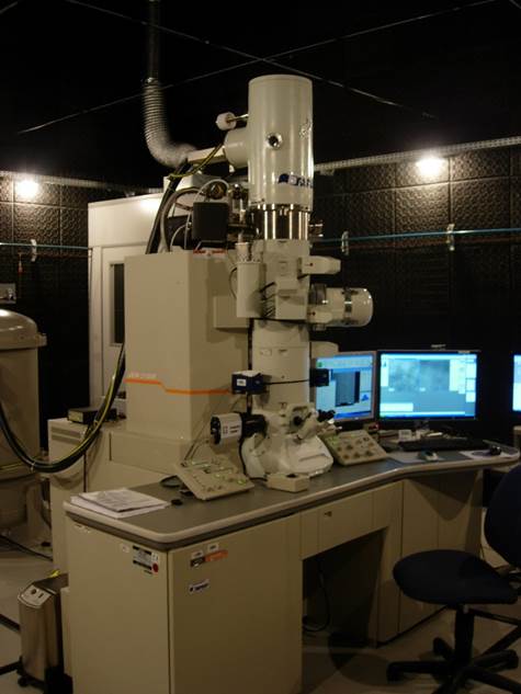
JEOL JEM-2100F
[slick-slider design=”prodesign-6″ show_read_more=”false” dots=”false” arrows=”false” autoplay=”false” category=”689″ include_cat_child=”false” exclude_cat=”370″ orderby=”title” order=”asc”]
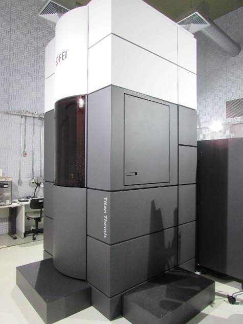
Thermo Fisher/FEI Titan Cubed Themis
Thermo Fisher/FEI Titan Cubed Themis
Thermo Fisher Scientific Quanta 650 FEG
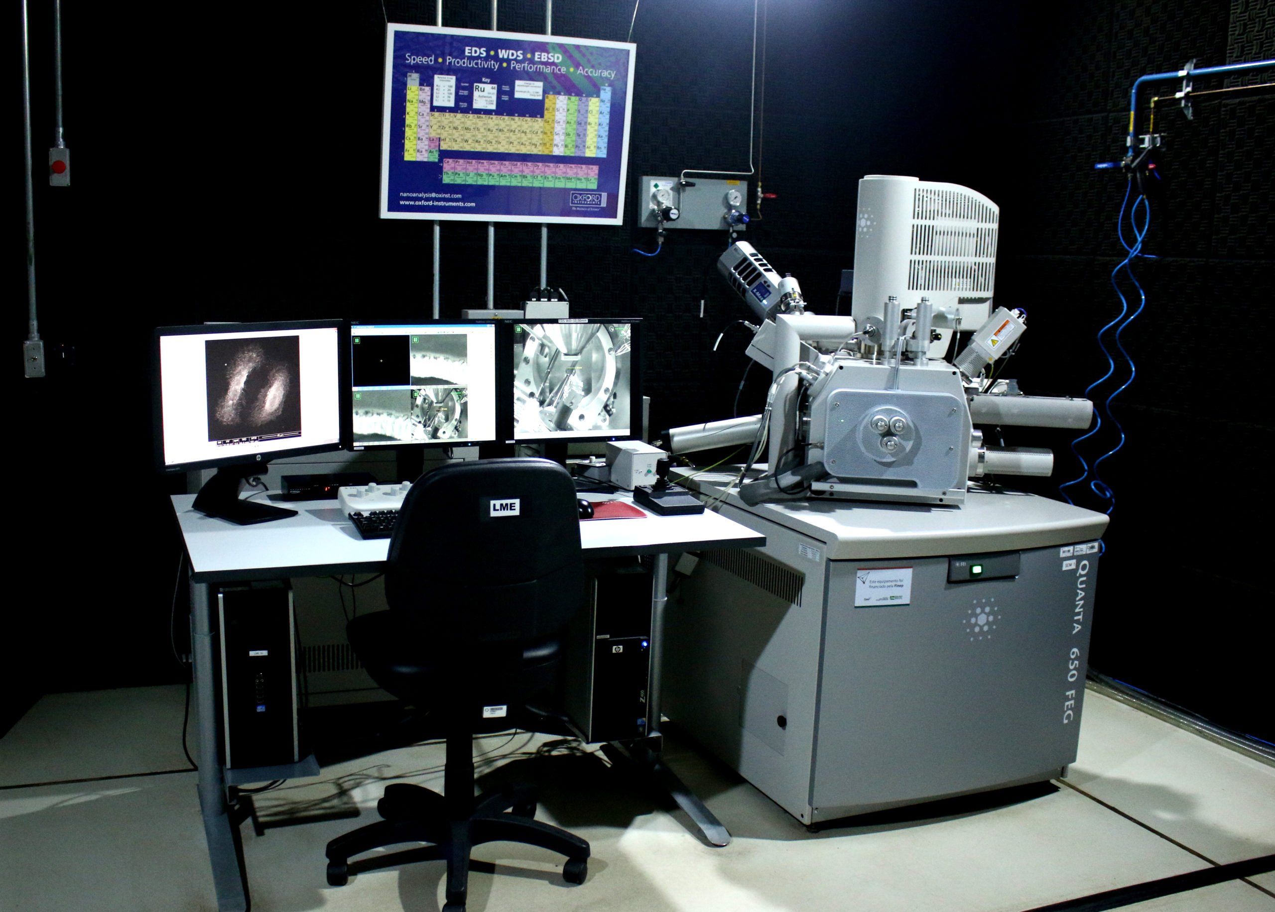
Thermo Fisher Scientific Quanta 650 FEG
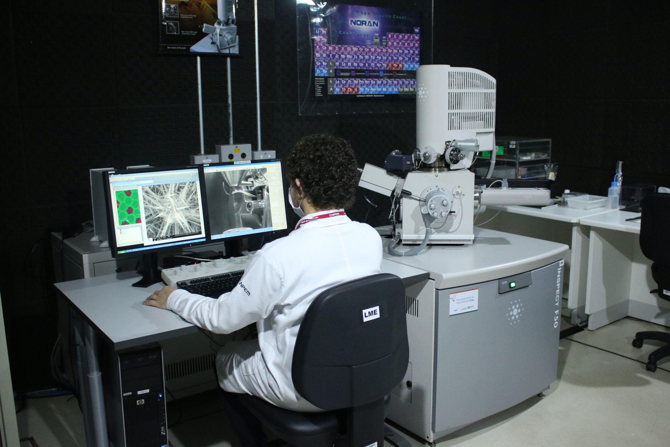
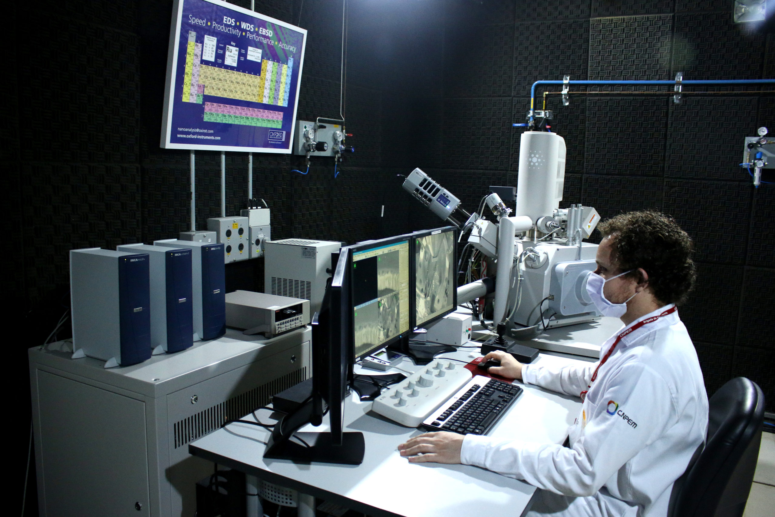
Thermo Fisher Scientific Inspect F50
Thermo Fisher Scientific Inspect F50
Thermo Fisher Scientific Helios NanoLab 660
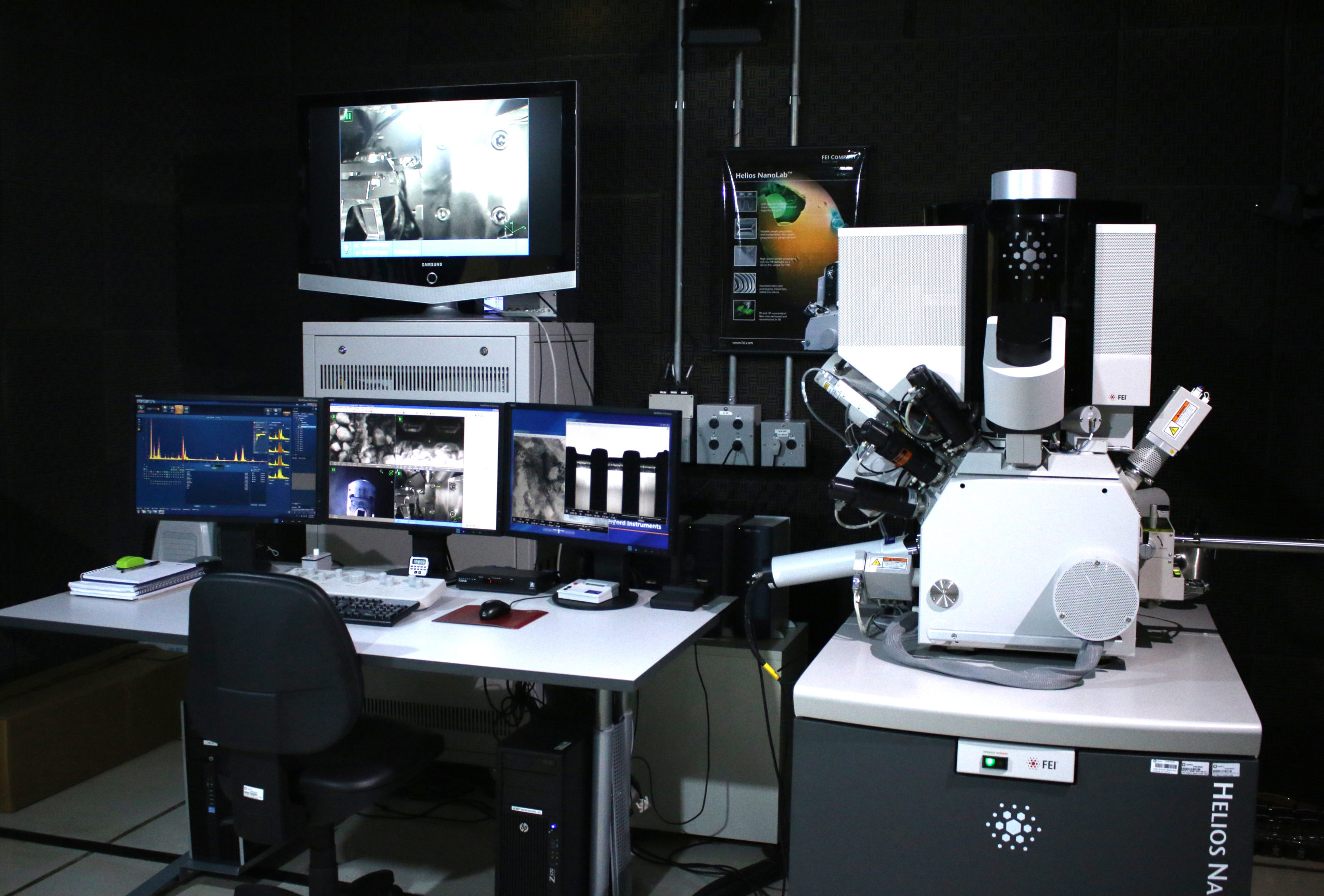
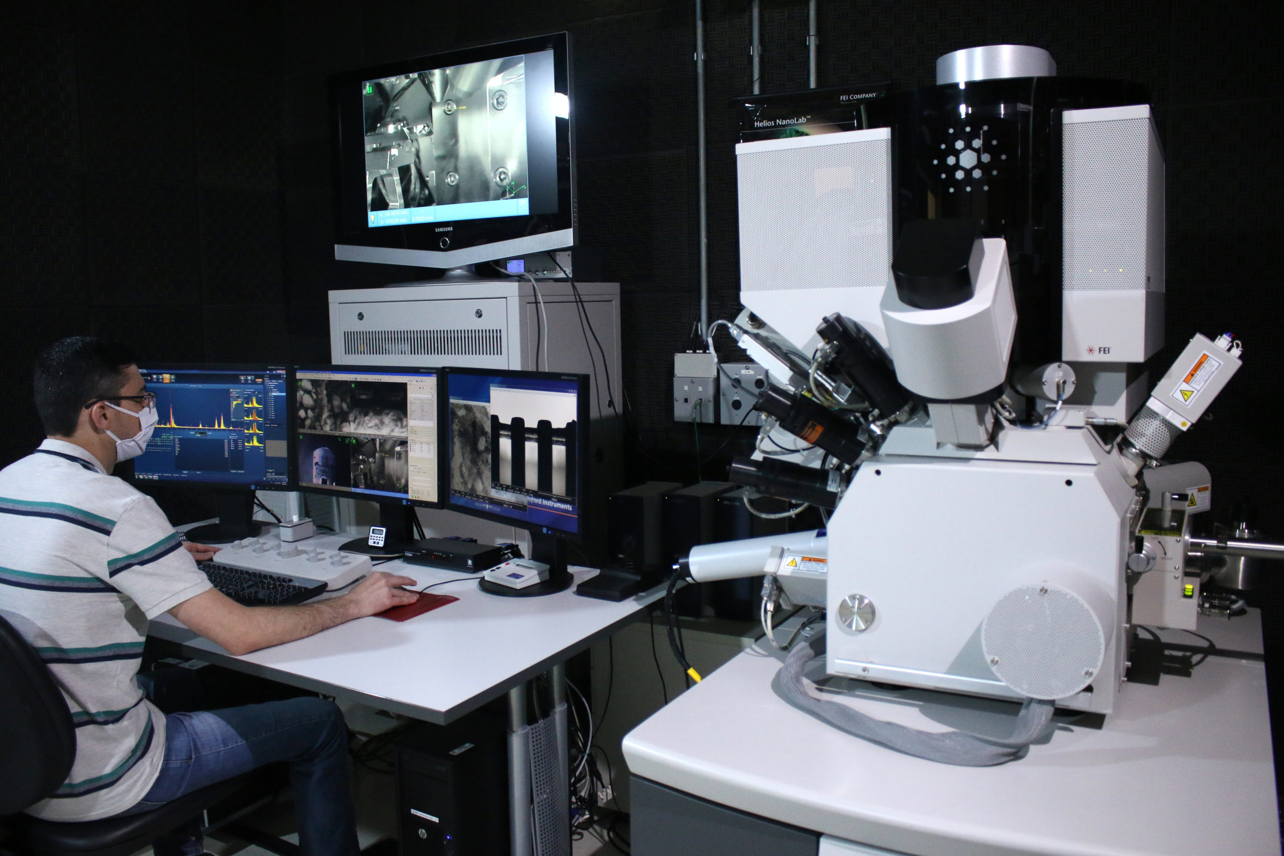
Thermo Fisher Scientific Helios NanoLab 660
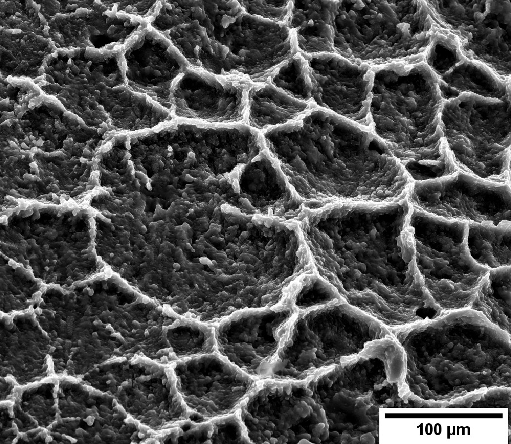
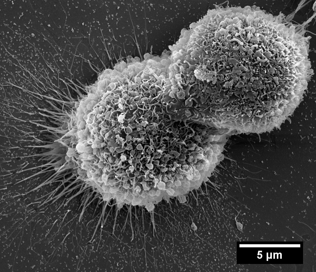
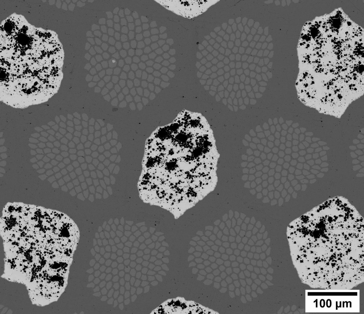
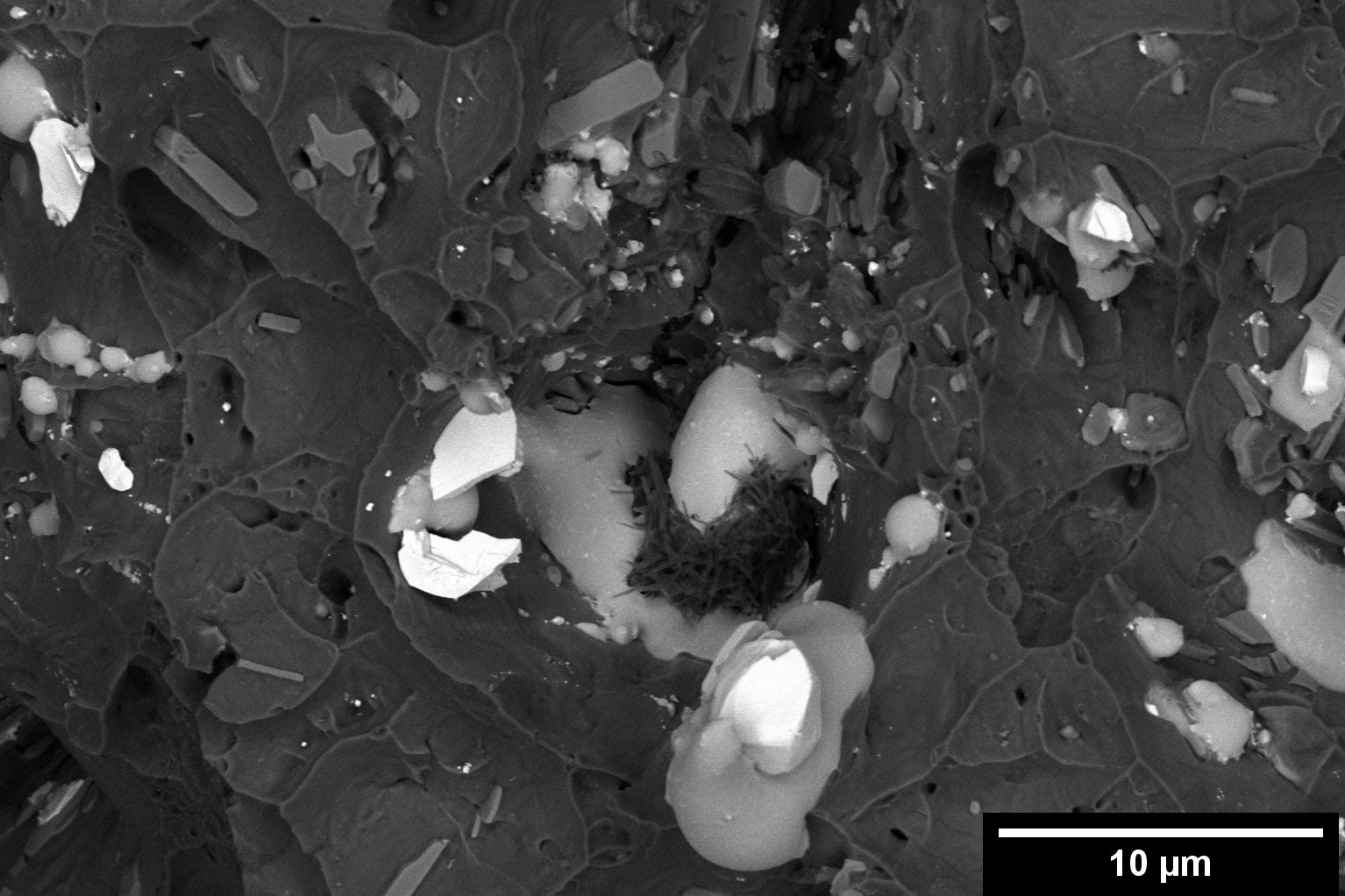
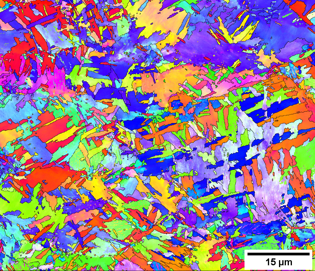
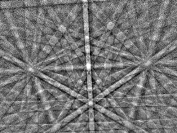
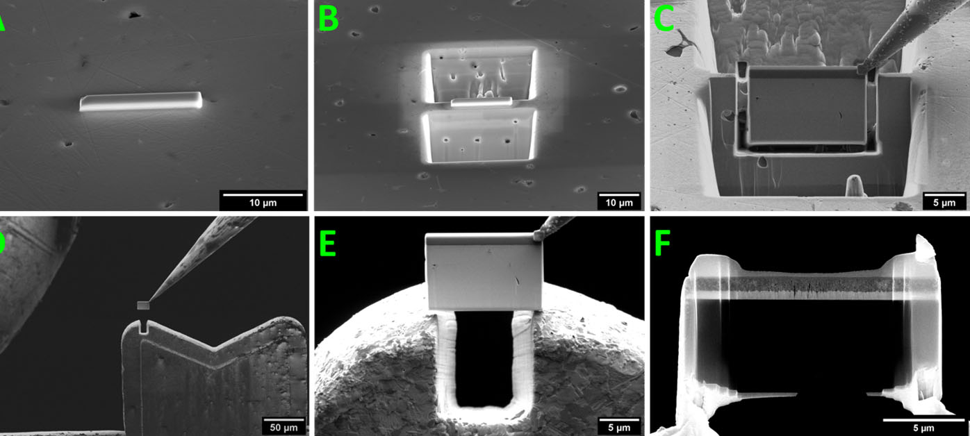
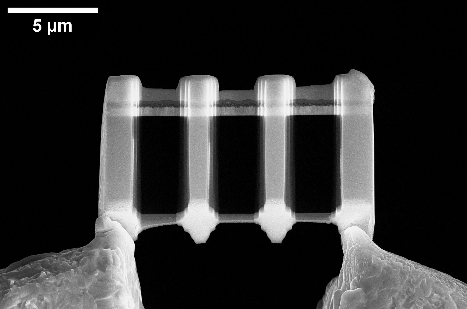
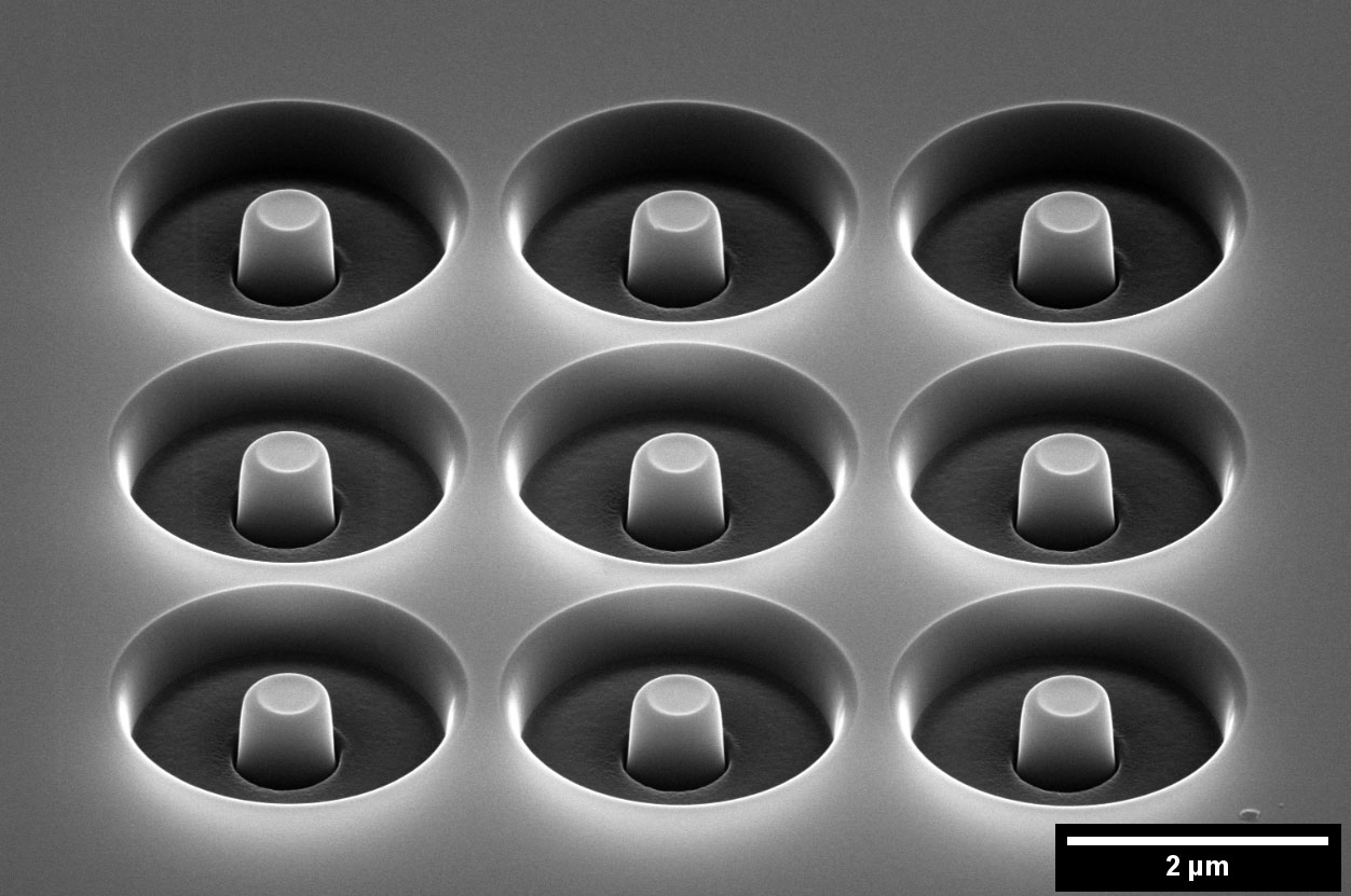
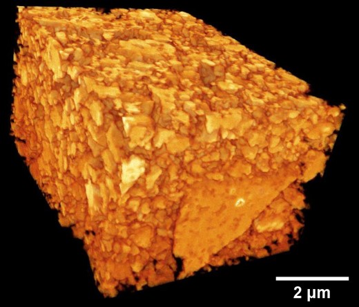
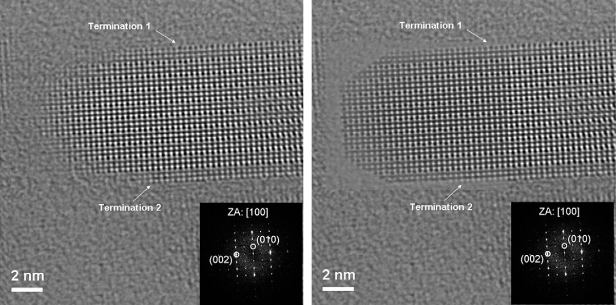
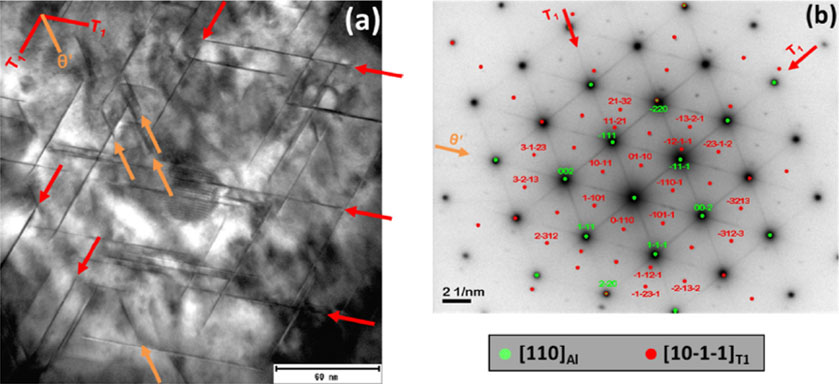
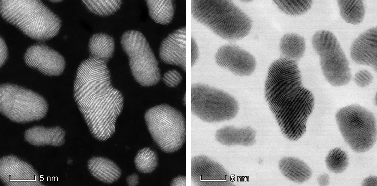
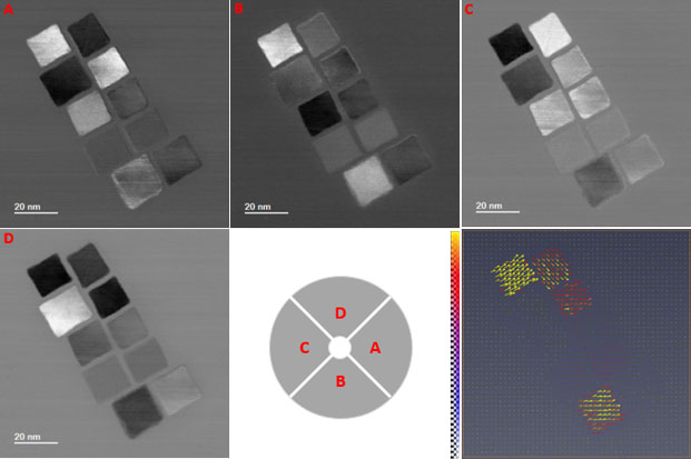
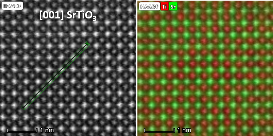
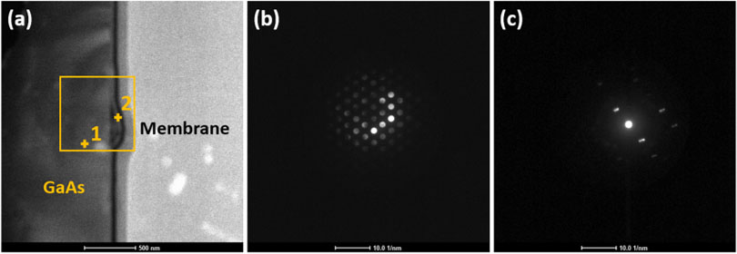
 Image gallery – Techniques and applications