
Physical deposition by ion bombardment – Sputtering
Sputter-type deposition is a moment transfer process in which atoms from a target are ejected or pulverized due to ion bombardment. The pulverized atoms travel until they reach a substrate, where they deposit to form the desired layer. As individual atoms, they are chemically active and quickly form compounds with the ions and atoms of the bombardment gas. For this reason, inert argon is used as a bombardment gas. For some applications, however, a reactive gas is purposely added to the argon so that the deposited film is a chemical compound rather than the elemental target materials. Spray deposition normally takes place at a pressure of 10-3 Torr. Therefore, the coating has a better conformation with the substrate geometry.
Physical deposition by electron beam – e-beam
Electron beam deposition takes place in a high vacuum (10-6 Torr). A focused beam of high-energy electrons is directed into a crucible containing the high-purity source material. The electrons that collide with the target heat the element until the phase change is solid-vapor, or solid-liquid-vapor. The steam flow is directed to the substrate, where it is condensed and deposited as a thin film. The high vacuum ensures highly directional deposit, which means that the film has more growth in the plane normal to the target.
MBE Technique
The MBE (molecular-beam epitaxy) technique refers to the process in which thin films or three-dimensional structures are formed on ordered and heated surfaces of monocrystalline substrates which, due to their characteristics as a network parameter and coefficient of thermal expansion, influence the formation of atomic arrangements. In this technique, the atoms or molecules come from solid sources with a high degree of purity, and can also be presented in a liquid state, as in the case of the chemical element gallium (Ga) used in the growth of compounds III-V. These charges are placed in effusion cells that are heated by power sources and monitored by PID controllers (proportional, integral and derivative) and, under ultra-high vacuum conditions (< 1.0 × 10⁻⁹ mbar), produce molecular beams with stable mass flow. Due to the rigor of the growing conditions, the MBE system makes it possible to produce films with high crystalline quality, in addition to accurately controlling the doping level (< 0.01 %), the film composition and the number of atomic monolayers. obtain multilayer heterostructures or two-dimensional films.
Equipment
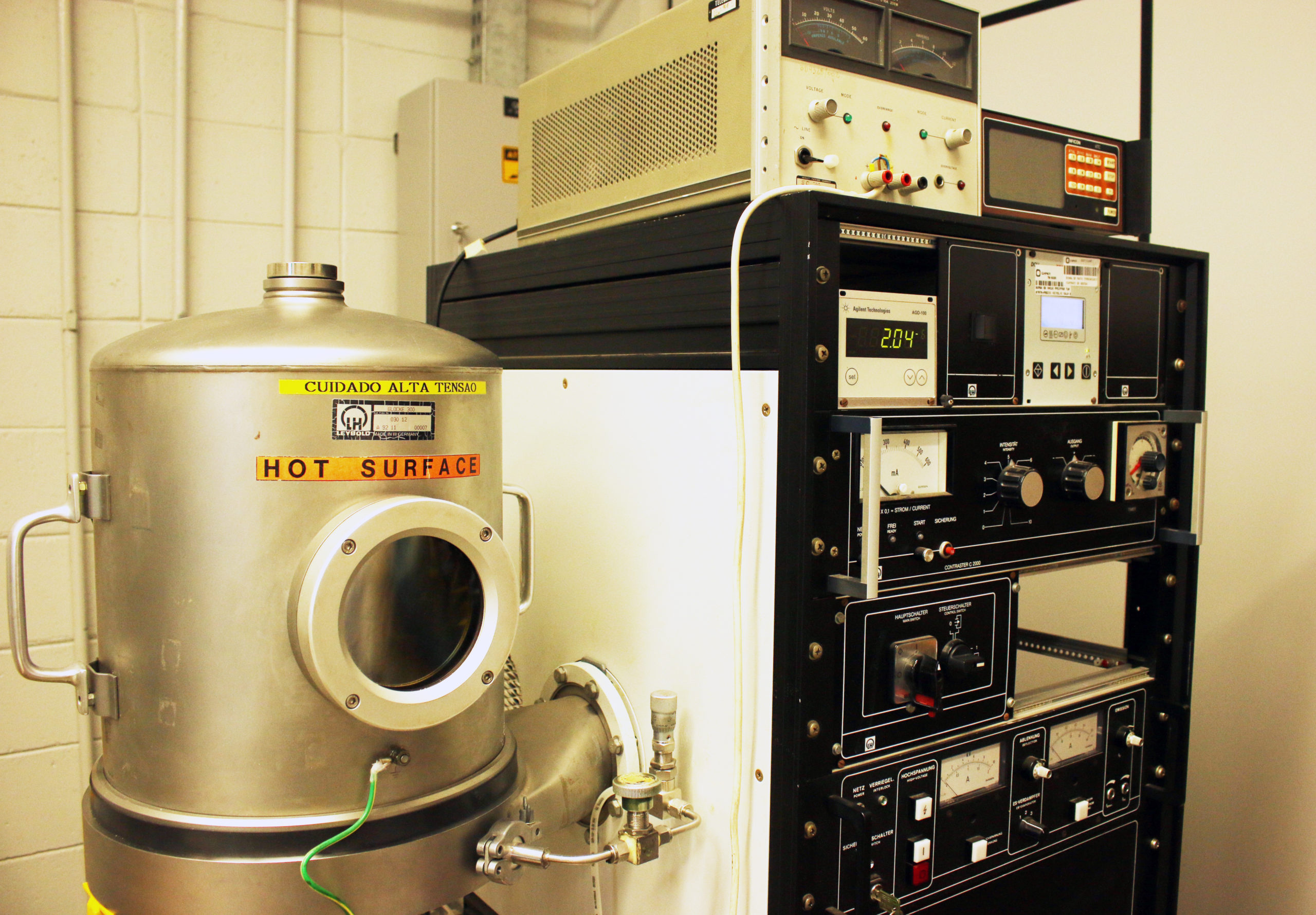
Electron beam deposition
- Source: 6 kV– 10 kV;
- Current: max. 190 mA;
- Sample size: ≤100mm;
- Heated sample holder: up to 500°C;
- Deposition chamber with capacity for up to 6 targets;
- Working pressure on the order of 1 x 10⁻⁷ Torr;
- Allowed materials: Cr, Au, Ti, Ni, Ag, NiFe, Ge, SiO, SiO2, among others upon request.
Electron beam deposition
- Sample size: ≤100mm;
- Deposition chamber with capacity for up to 4 targets;
- Working pressure on the order of 1 x 10⁻⁶ Torr;
- Two sources for simultaneous deposition of two materials (deposition rate control only monitors one at a time);
Allowed materials: Pc (Phthalocyanine), CuPc, CoPc, FePc, F16CuPc, among others upon request.
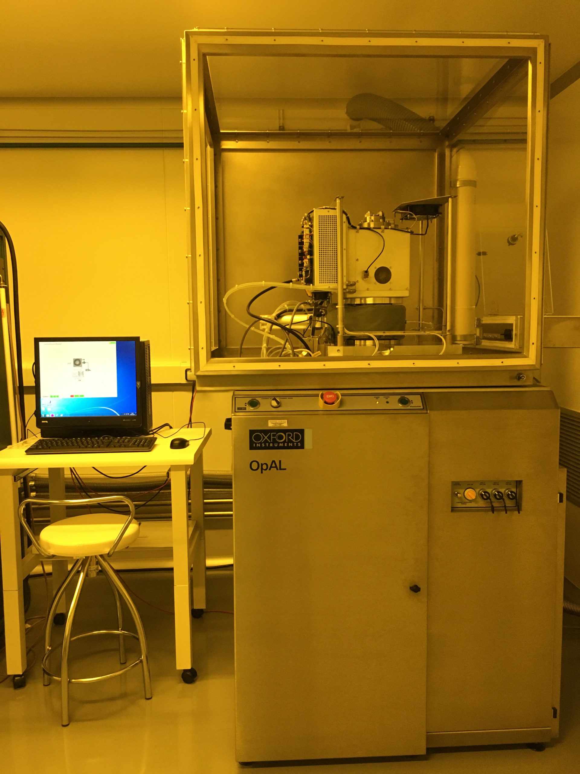
Atomic layer deposition
- Sample size: ≤ 100mm.
- Available processes:
- Al2O3 – Thermal deposition (TMA precursor);
- TiO2 – Plasma Deposition (TTIP Precursor); Deposition chamber with capacity for up to 6 targets;
- Working pressure on the order of 1 x 10⁻⁷ Torr;
- Allowed materials: Cr, Ti, Ni, Ag, NiFe, Ge, SiO, SiO2, among others upon request.
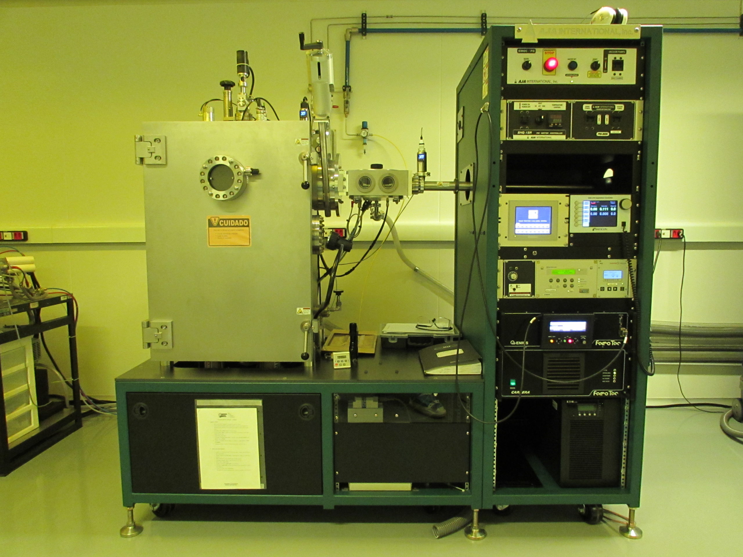
Sputtering deposition
- Source: DC
- Sample size: A few mm up to 6 x 177 mm wafers.
- High density plasma beam;
- Allows reactive sputtering: O2 and N2 gases;
- 4 manual rotating targets;
- Working pressure in the order of 8 x 10⁻⁷ mbar;
- Allowed materials: Cr, Au, Ti, Ni, NiFe, Al, Cu, Pt, Pd, Wti, among others upon request.
Electron beam deposition
- Source: 4 kV;
- Current: max. 190 mA;
- Sample size: ≤100mm;
- Deposition chamber with capacity for up to 2 materials; Working pressure in the order of 1 x 10⁻⁶ mbar;
- Allowed materials: Cr, Au, Ti, Al, Ni, Pt, Fe, SiO2 among others, on request.
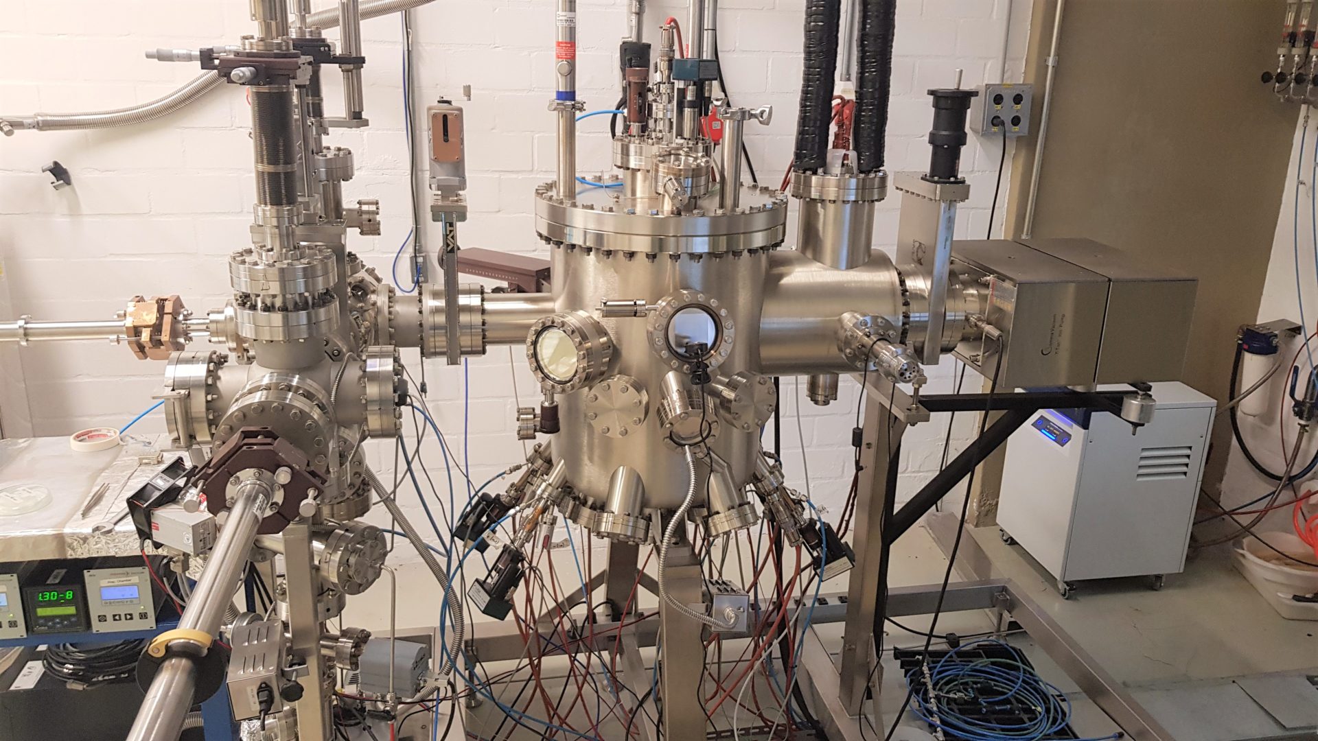
Epitaxial growth system – MBE III-V
- Bottom pressure: ~ 1 × 10⁻¹⁰ mbar;
- Sources: arsenic (As), gallium (Ga), silicon (Si), aluminum (Al), indium (In);
- 15 kV High Energy Reflected Electron Diffraction (RHEED) system integrated with iRHEED data acquisition system;
- Hydrogen beam for substrate surface cleaning;
- Substrate size: maximum 2” diameter
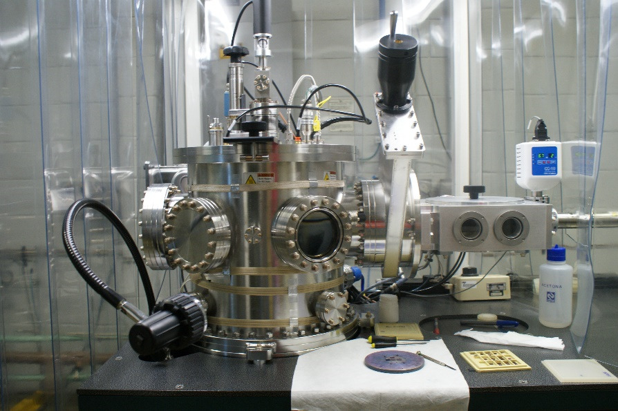
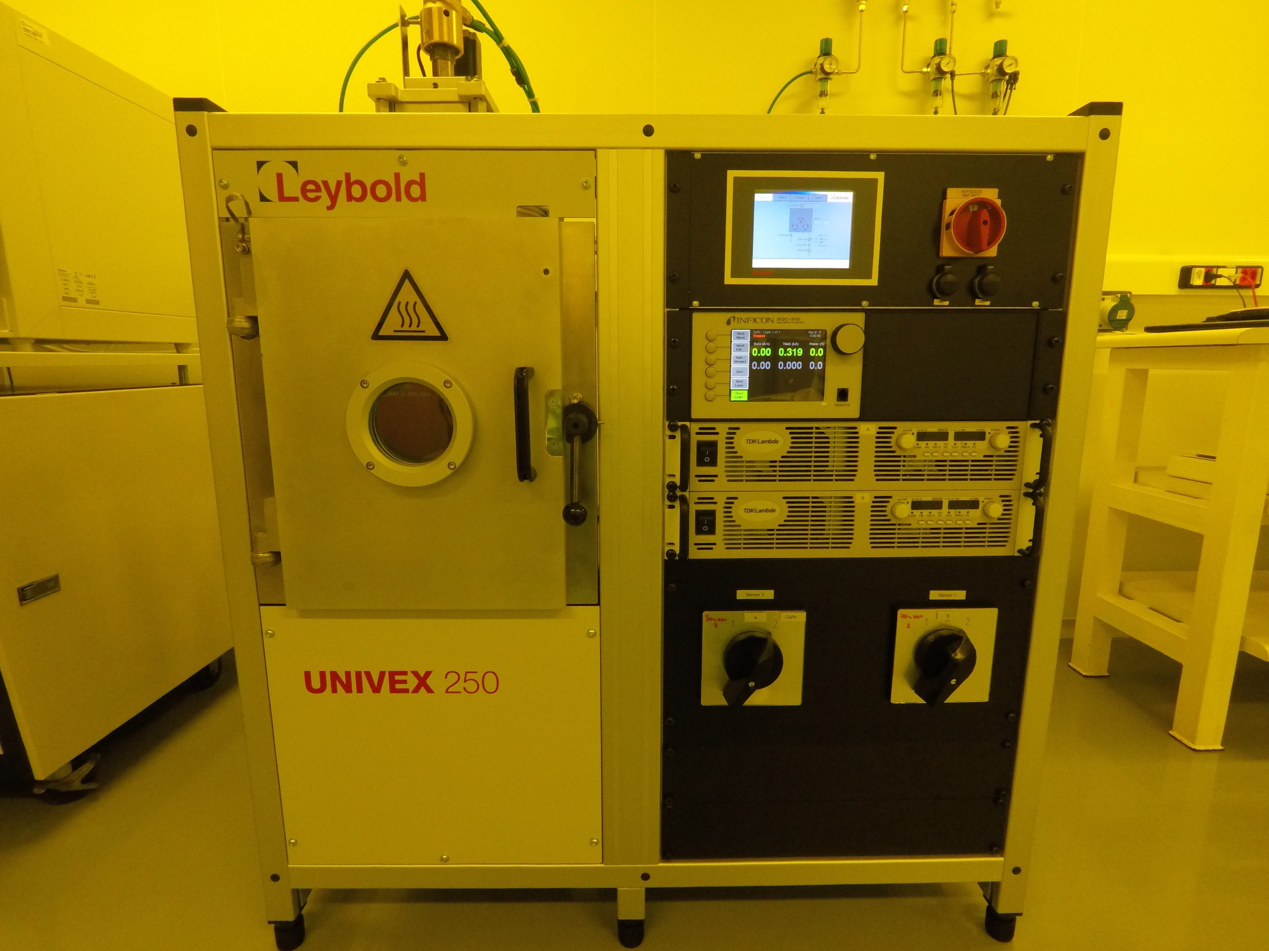
Sputtering deposition
- Source: DC/RF
- Sample size: up to 76 mm.
- Sample holder heating: up to 600°C;
- Target-Substrate Distance: Variable;
- Fully computer controlled;
- Loading chamber separate from main;
- Independent deposition of up to 5 simultaneous materials;
- Allows reactive sputtering: O2 and N2 gases
- 6 confocally mounted targets
- Working pressure in the order of 2 x 10⁻⁸ Torr
- Allowed materials: Cr, Au, Ti, Ni, NiFe, Al, Cu, Pt, Pd, Wti, Fe, Si, Ge, SiO2, TiO2, among others upon request.
For Au depositions, user’s contribution is required.
Equipment
Electron beam deposition
- Source: 6 kV– 10 kV;
- Current: max. 190 mA;
- Sample size: ≤100mm;
- Heated sample holder: up to 500°C;
- Deposition chamber with capacity for up to 6 targets;
- Working pressure on the order of 1 x 10⁻⁷ Torr;
- Allowed materials: Cr, Au, Ti, Ni, Ag, NiFe, Ge, SiO, SiO2, among others upon request.
Electron beam deposition
Sample size: ≤100mm;
Deposition chamber with capacity for up to 4 targets;
Working pressure on the order of 1 x 10⁻⁶ Torr;
Two sources for simultaneous deposition of two materials (deposition rate control only monitors one at a time);
Allowed materials: Pc (Phthalocyanine), CuPc, CoPc, FePc, F16CuPc, among others upon request.
Atomic layer deposition
Sample size: ≤ 100mm.
Available processes:
Al2O3 – Thermal deposition (TMA precursor);
TiO2 – Plasma Deposition (TTIP Precursor); Deposition chamber with capacity for up to 6 targets;
Working pressure on the order of 1 x 10⁻⁷ Torr;
Allowed materials: Cr, Ti, Ni, Ag, NiFe, Ge, SiO, SiO2, among others upon request.
Sputtering deposition
Source: DC
Sample size: A few mm up to 6 x 177 mm wafers.
High density plasma beam;
Allows reactive sputtering: O2 and N2 gases;
4 manual rotating targets;
Working pressure in the order of 8 x 10⁻⁷ mbar;
Allowed materials: Cr, Au, Ti, Ni, NiFe, Al, Cu, Pt, Pd, Wti, among others upon request.
Electron beam deposition
Source: 4 kV;
Current: max. 190 mA;
Sample size: ≤100mm;
Deposition chamber with capacity for up to 2 materials; Working pressure in the order of 1 x 10⁻⁶ mbar;
Allowed materials: Cr, Au, Ti, Al, Ni, Pt, Fe, SiO2 among others, on request.
Sputtering deposition
Source: DC/RF
Sample size: up to 76 mm.
Sample holder heating: up to 600°C;
Target-Substrate Distance: Variable;
Fully computer controlled;
Loading chamber separate from main;
Independent deposition of up to 5 simultaneous materials;
Allows reactive sputtering: O2 and N2 gases
6 confocally mounted targets
Working pressure in the order of 2 x 10⁻⁸ Torr
Allowed materials: Cr, Au, Ti, Ni, NiFe, Al, Cu, Pt, Pd, Wti, Fe, Si, Ge, SiO2, TiO2, among others upon request.
For Au depositions, user’s contribution is required.