The technique of optical lithography or photolithography uses ultraviolet (UV) radiation to sensitize a photosensitive resin, known as photoresist. During the development step, areas radiated by light are removed, creating a binary profile on the substrate (with and without photoresist).
The main components of the photoresist are: polymer (base resin), sensitizer and solvent. After exposure to radiation with a specific wavelength, the polymer changes the size of the structural chain through new bonds or breakage of molecules. In the case of positive photoresists, where light is radiated, fragmentation of the molecular chain occurs, leaving this region with a higher dissolution rate than the other shaded regions. With negative photoresists, however, the opposite occurs, the regions that were affected by light trigger a reaction that increases the size of the chain, a process known as crosslinking. Thus, these regions are dissolved at a lower rate than the other areas not sensitized by light.
Two techniques are available for exposing patterns: masked and unmasked (rapid prototyping). In the first case, a transparent substrate containing regions that allow the passage of light and regions protected with metal (preventing the passage of light) is used, also known as a photomask. In the case of rapid prototyping, a system uses projection lenses combined with micrometer-accurate scanning engines to selectively expose regions of the substrate, without the need for a physical mask. Standards for direct projection are defined by a virtual mask previously designed in dedicated software.
Equipment
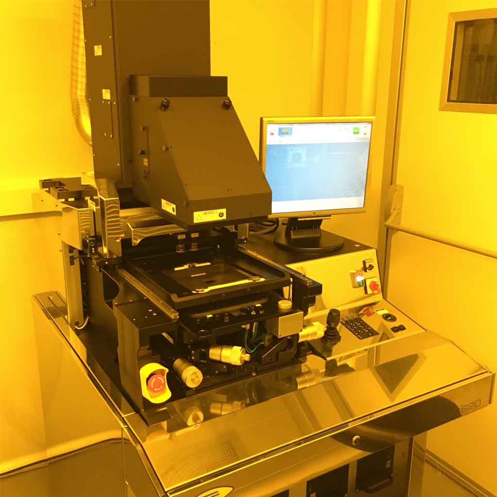
Mask Aligner – EVG620 Series (EV Group)
- Source: High Pressure Mercury Lamp. Power 500 W. Spectrum from 365 nm to 405 nm;
- Substrate size: up to 100mm diameter wafers;
- Requires photolithography masks;
- Minimum resolution 2 µm *
* Under specific process conditions
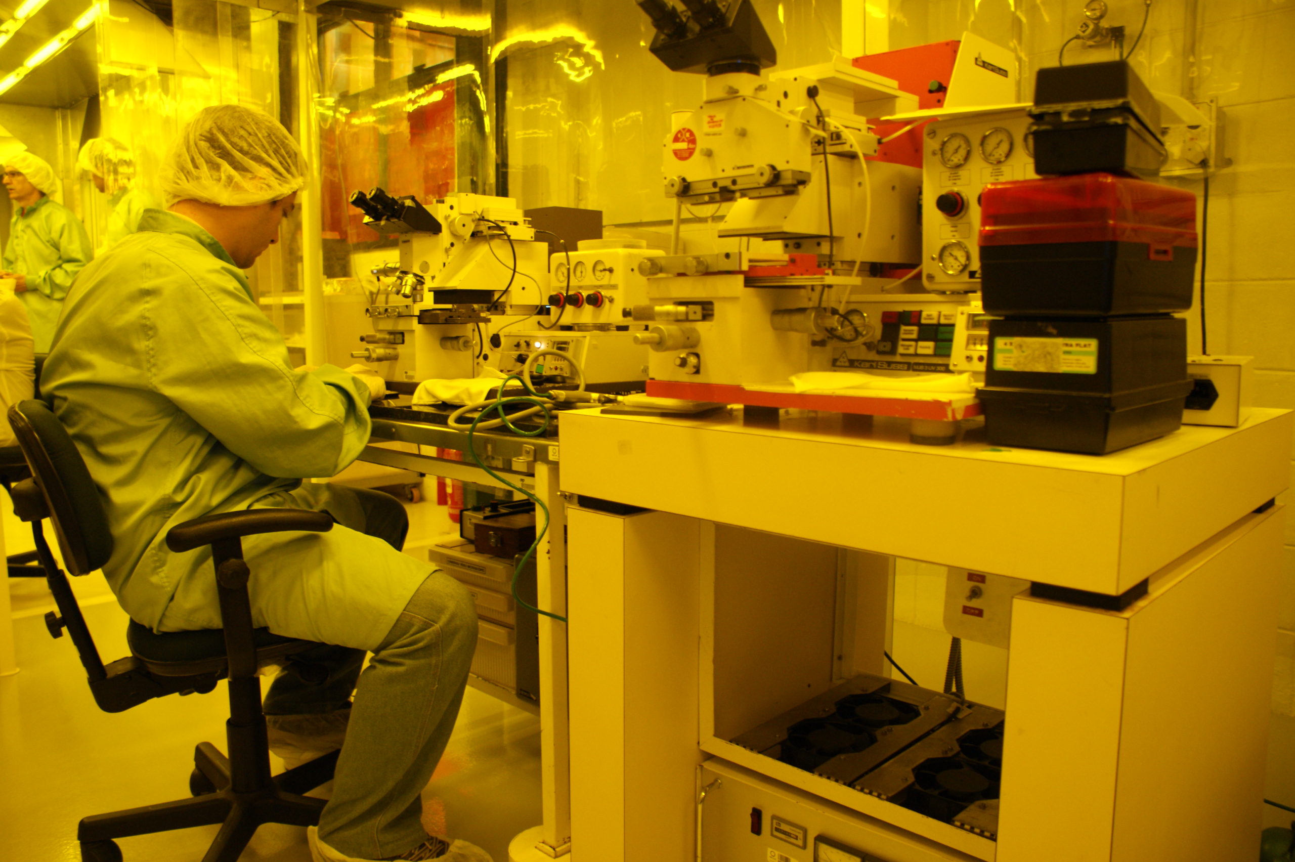
Mask Aligner – MJB3 (Karl Suss)
- Source: High Pressure Mercury Lamp. Power 350 W. Spectrum from 365 nm to 405 nm;
- Substrate size: up to 75mm diameter wafers;
- Requires photolithography masks;
- Minimum resolution 2 µm *
* Under specific process conditions
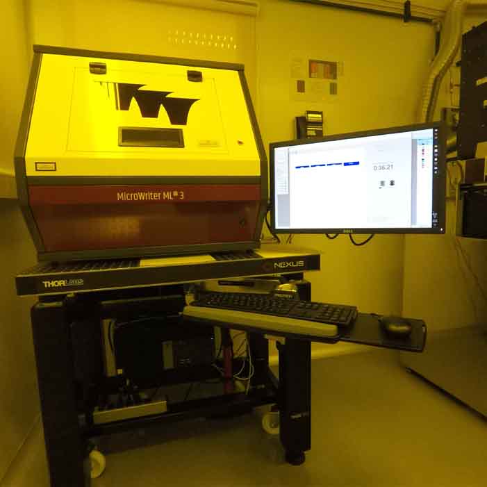
Direct Prototyping – ML3 (DMO)
- Source: High power laser with 405 nm, 365 nm and 385 nm spectrum;
- Substrate size: up to 100mm diameter wafers;
- Lenses available for 1 µm, 2 µm and 5 µm resolution.
- Partially open to users
We do not offer lithographic masks
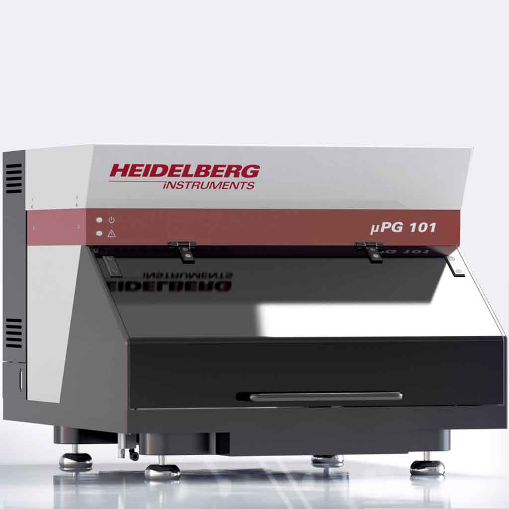
Direct Prototyping - µPG 101 (Heidelberg Instruments)
- Source: High power laser with 405 nm spectrum;
- Substrate size: up to 100mm diameter wafers;
- Resolution: 5 µm.
We don’t offer lithographic masks
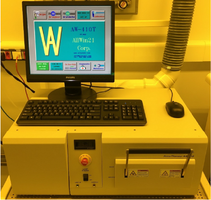
RTP oven for heat treatment AW 410 (AllWin corp.)
- Substrate size: Min. 9mm x 9mm up to 100mm diameter wafers;
- Temperature: 400 – 1,200 °C;
- Available gases: Air, N2, O2, H/Air Mix (5%/95%)
System dedicated to processes in Silicon
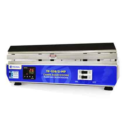
Chapa aquecedora para tratamento térmico Tecnal
Temperatura : Até 250 °C.